Running Custom Code on a Google Home Mini (Part 1)
Posted on Sat 25 July 2020 in Projects
Introduction
As demonstrated in the previous articles of this website, I’ve always been interested in running my own code on consumer devices.
In this series of two articles, we’ll take a look at the well-known Google Home Mini.
To achieve this goal, we’ll have to go rather deep into the rabbit hole. Various topics and techniques will be explored.
Google Home Mini Hardware Overview
First things first, let’s start with a general overview of the Google Home Mini Hardware.
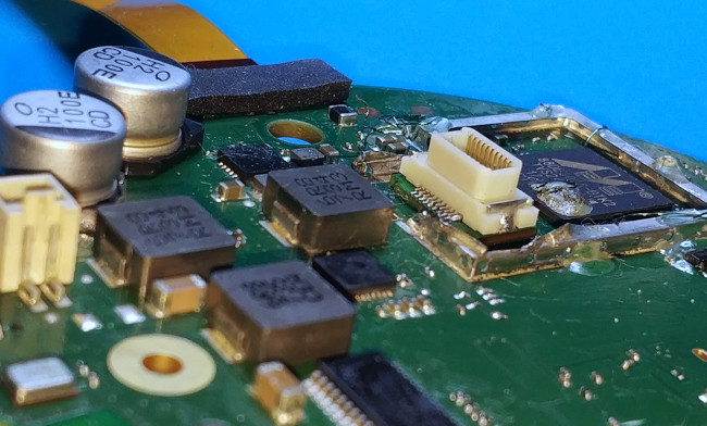
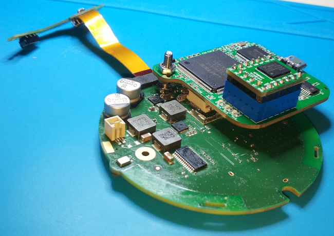
Cracking the case open reveal the following PCB. Important components are all annotated. Some RF shields have been removed to expose the components.
The main Google Home Mini MPU. It's a ARM-based SoC manufactured by Marvell and branded as "ARMADA 1500 Mini Plus".
A TC58NVG1S3HBAI6 256 MB NAND Flash. It contains the entire firmware of the Google Home Mini
This push button is not accessible without cracking the case open. Pushing it at boot time will force the bootloader to boot from the USB port of the device. However, only signed code can theoretically be executed.
One of the two MEMS microphone of the device. The acoustic hole is on the other side of the PCB.
One of the two MEMS microphone of the device. The acoustic hole is on the other side of the PCB.
The main speaker of the Google Home can be plugged to this two pins connector.
A LED Driver. It communicates with the MPU via an i2c bus.
An audio CODEC, driving the main speaker. It communicates with the MPU via i2c and I2S buses.
A DDR memory, used by the main processor.
A WLAN/BT module, manufactured by Marvell.
A mechanical switch, used to disable and enable the microphones.
A micro USB port. It provides power to the entire system. Data lines are also routed to the main processor.
Quick side note: So far, I have opened two Google Home Mini. On these two units, the NAND Flash component used isn’t the same. However, to keep things simple, this article will expect a TC58NVG1S3HBAI6 flash to be used all along.
Most components are BGA components. It makes reverse-engineering the system harder: difficult for instance to probe individual signals between two integrated circuits. Further, reliably reworking the board (i.e., desoldering and soldering back a component) requires quite some skills.
I didn’t find any active JTAG interface during my research. The same goes for debug UART test points.
Finally, it’s important to note that the main CPU comes without public documentation. Very few details about this component are available online. All the juicy technical data is likely protected by a NDA.
To conclude, at first sight, the hardware looks rather annoying to work with and doesn’t appear to be very talkative.
Past Studies
As you might expect, I’m not the only one who has been studying the Google Home devices. Here is a quick summary of what others have discovered at the time of writing of this article.
Chromecast Vulnerabilities
The hardware and software of the Google Home Mini is very close to what is embedded into Google Chromecast devices. Hence, it’s interesting to take a look at what has already been discovered against this product.
In 2014, fail0verflow was able to root Chromecast devices with a vulnerability affecting the bootloader. A buffer overflow vulnerability triggered thanks to a special USB peripheral led to a full secure boot bypass. The vulnerability is detailed here and there.
The vulnerability has now been patched and the Google Home family was never impacted by the issue.
However, the work from fail0verflow has two interesting takeaways for us:
- Many eyes already took a look at the bootloader. It’s reducing the likelihood I can still discover something to exploit in it to bypass the secure boot on a Google Home Mini.
- The articles highlight that Google has released the source code for the bootloader and Linux Kernel running on the Chromecast. The same goes for the Google Home family. Everything is available here. This source code will be extremely useful in the second article of this series.
DEFCON27 Presentation
Another essential piece of information is the presentation given during DEFCON27 untitled “Breaking Google Home: Exploit It with SQLite(Magellan)”. The slides are available here.
In the presentation, an attack impacting the userspace software of the Google Home is detailed. This led to the result I want to achieve: code execution on the Google Home.
While extremely informative, the attack described by the presentation cannot be used against my own device anymore. The bugs have all been patched already.
However, the presentation contains an interesting slide that summarizes quite well what the attack surface of the Google Home Mini is.
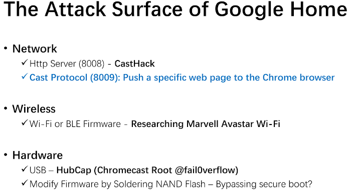
The fail0verflow work is shown, as well as possible network attacks that are explored in the presentation.
What’s left is to research vulnerabilities in the Wi-Fi/BLE module of the device or to modify the firmware stored in the NAND Flash of the device.
My Own Goal
These studies make very clear that:
- The Google Home Mini is protected by some kind of secure boot. The Bootloader and Kernel are cryptographically verified.
- Many interesting attack vectors have already been explored.
Considering this, I chose to go the NAND Flash way.
My goal will be to modify the NAND flash content until I can execute my own code.
“What’s the point?” you might ask. Well, here are a few reasons:
- It’s the most direct way of achieving code execution on the platform.
- Dynamic analysis of the Goggle Home software running on the actual hardware becomes possible.
- Similarly, it may be useful to explore the Wi-Fi/BT module attack vector.
- As explained before, the SoC of the Google Home Mini comes without any public documentation. Being able to run custom code on it is valuable to understand it better. Things like dumping the BootROM of the system become possible.
- Last but not least, it’s an interesting challenge that will need me to go down the rabbit hole. The content and structure of the NAND Flash will need to be understood. An exploit could be needed to bypass the secure boot.
This path may sound like the easiest way to go to achieve code execution, but an important challenge will first have to be addressed.
Indeed, as I explained in the previous section, the hardware design of the Google Home Mini is not “rework friendly” at all.
The NAND Flash is a BGA component. Desoldering and soldering it back is easier said than done, especially considering I’ll likely have to do it multiple times. Some little tricks will need to be used.
The NandBug System
General Concept Idea
Repeatedly desoldering and soldering back the NAND Flash would have been annoying and could have caused damage to the PCB.
Manually soldering thin wires to the BGA footprint for breaking out the NAND Flash lines could have been risky because of signal integrity issues. It wouldn’t have been a very clean and, more importantly, reliable solution.
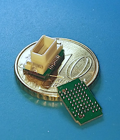
Hence, to overcome this burden, I developed NandBug.
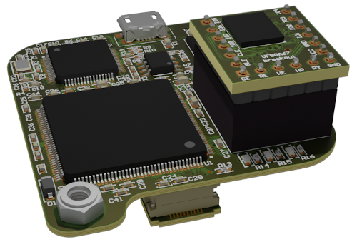
NandBug is composed of three boards:
- The Interposer Board that’s soldered to the Google Home Mini PCB, right at the NAND Flash location. This board breaks out the NAND Flash signals to a tiny connector.
- The Main Board, that can be connected to both the Interposer Board and Daughter Board. It can communicate with a computer through a USB interface.
- The Daughter Board. The delicate BGA NAND Flash IC is soldered to this board.
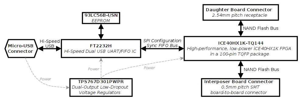
The general concept of NandBug is described by the following diagram.
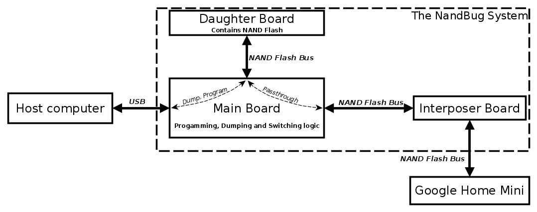
In a word, thanks to this system, the NAND Flash IC can be accessed from both the Google Home circuit and the electronic of the Main Board.
The general idea is in fact to make the NAND Flash of the Google Home in-system programmable. It may sound like an overengineered solution, and it maybe is. But, hey, I’m doing this project for fun anyway.
I made the schematics, Gerber files, and software of NandBug publicly available.
Hardware files are available here, while the software can be downloaded from here.
Technical details concerning NandBug will now be given in the following sections.
NandBug Hardware Overview
The NandBug Main Board
Schematics and manufacturing files for this board are available here.
A block diagram is available below.
The main NandBug Board is PCB is detailed in the following picture.
An ICE40 FPGA.
A FT2232H. This component adds Hi-Speed USB connectivity to the board.
An EEPROM. It contains configuration data for the FT2232H.
A dual output low dropout voltage regulator, used to provide power to the FPGA.
Three general purpose red LEDs and associated current-limiting resistors
Connector for the daughter board PCB. Optionally, a NAND Flash can be directly soldered to the board.
A micro-USB connector, used for power and data transfer.
The Interposer Board Connector.
The main component of this board is a ICE40HX1K-TQ144 FPGA. This component has been chosen for the following reasons:
- It’s reasonably priced.
- Its bitstream format has been reverse-engineered, and it is now supported by open source toolchains.
This FPGA can be configured in different ways: dumping the NAND content as well as programming it is possible. It can also be configured as a pass-through to let the Google Home Mini access to the NAND Flash directly.
A FT2232H is connected to the FPGA. This component adds USB connectivity to the main board and serves two purposes:
- Sending various configuration bitstreams to the FPGA. This is done by using the SPI protocol and a couple of additional GPIOs.
- Receiving and transmitting data to and from the NAND Flash. This is done using the Synchronous FIFO mode of the
FT2232H. In this mode, the FPGA and theFT2232Hcommunicates by using a parallel bus synchronized by a 60Mhz clock. This allows for a reasonably fast data throughput. The entire content of the 256 MB NAND can be dumped in less than a minute. The 60MHz clock is generated by theFT2232H, and clocks the entire FPGA.
I, personally, find this combination of a FT2232H and ICE40HX1K-TQ144 to be quite interesting and versatile. I’ll for sure use it again in future projects. However, please note that using both the SPI mode and Synchronous FIFO mode of the FT2232H requires adding an EEPROM to the BOM. This EEPROM contains configuration data for the FT2232H and can sometimes be omitted.
On the bottom side of the board, only the Interposer Board connector is fitted.
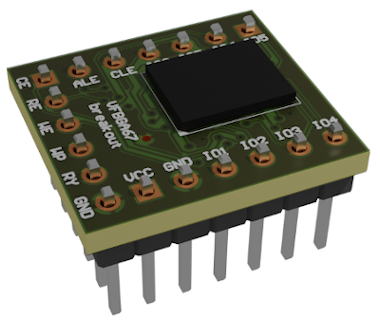
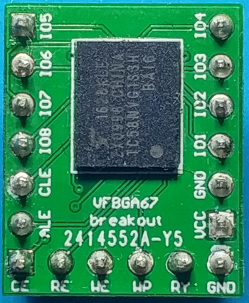
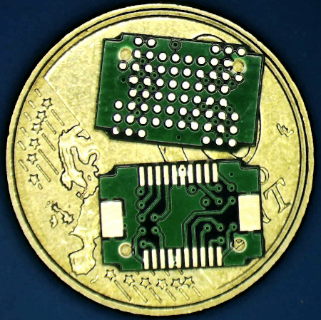
The Daughter Board
Schematics and manufacturing files for this board are available here.
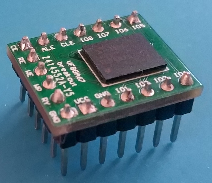
There isn’t much to say about this board. It’s simply breaking out the NAND Flash signals to traditional 2.54 mm pitch connectors.
The rationale behind this design choice is that I didn’t want to solder the NAND Flash directly to the Main Board for two reasons:
- I’m not super confident in my BGA reworking skills.
- It makes swapping NAND Flash component faster and easier.
Of course, using 2.54 mm connectors may cause signal integrity issues when dealing with high-speed signals. However, looking at the Flash datasheet, it appears the maximum speed was not that fast, and I chose to take the risk.
The Interposer Board
Schematics and manufacturing files for this board are available here.
The Interposer Board is rather simple and is only composed of two things:
- A small connector matching the one from the main board.
- A footprint for the NAND Flash. It’s a mirrored version of the “normal” NAND Flash schematic. Indeed, this board will be soldered in place of the original NAND on the Google Home Mini PCB.
This board is obviously pretty simple, just a bunch of wires. What has been a challenge was to install it on the Google Home Mini.
A quick note on Manufacturing
All these boards have been manufactured for cheap by JLCPCB.
The Main Board has been partially assembled by their SMT assembly service. I only had to hand solder the USB connector, interposer connector and FPGA.
Installing NandBug on the Google Home Mini
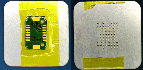
Removing the NAND Flash from the Google Home PCB
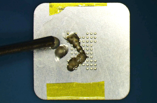
First things first, the NAND Flash must be desoldered from the Google Home PCB. This has been done with a cheap hot air reworking station. It’s a model that can be bought from many places and that has served me well for several years now.

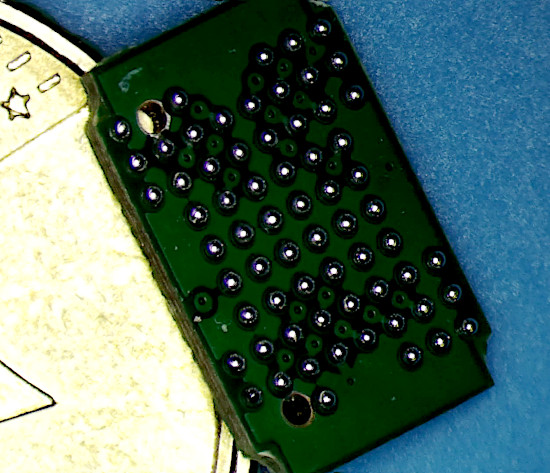
The desoldered NAND Flash must be kept. It must be soldered to the Daughter Board. Soldering it to this board follows the usual BGA reworking procedure: using a lot of solder flux and hot air.
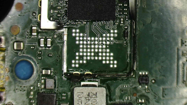
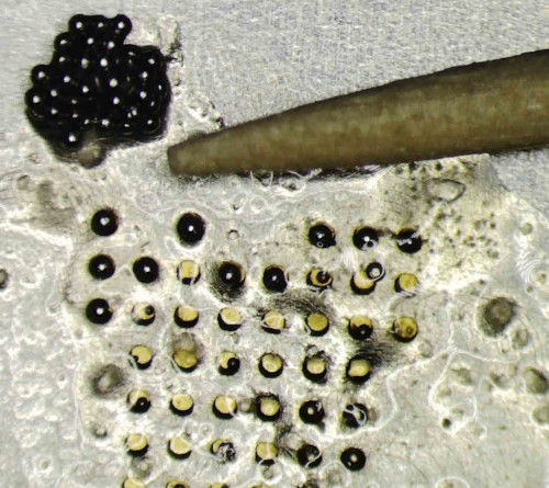
Next, on the Google Home Mini PCB side, the BGA footprint must be cleaned for the Interposer Board to sit flush against the PCB.
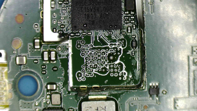
This is done with a soldering iron equipped with a flat tip, a small piece of desoldering braid and a lot of soldering flux.
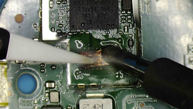
After the operation, here is the result.
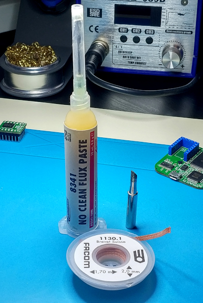
Preparing the Interposer Board
It’s now time to prepare the Interposer Board.
As it must be soldered like a BGA component, I’ll turn it into one by soldering tiny solder balls.
Such solder balls can be bought online. I’m using a diameter of 0.4 mm.

To help with the soldering process, I ordered a stencil at the same time as the Interposer PCB. The holes of the stencil are matching the NAND Flash footprint.
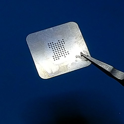
The naked Interposer PCB can be duct-taped against this stencil. Heat-resistant Kapton tape is used.
Next, a good amount of flux is dispensed. It must fill the holes.
Here comes the most tedious step: placing one tiny 0.4 mm ball per hole. A simple toothpick is used to drag them to the right places.
Everything is next melted together with the hot air station. For the record, I’ve tried to shoot a video of this procedure, but the optics and image sensor of my stereo microscope being super sketchy, the resulting video quality is absolutely terrible. You can still find it here. A better video of a similar process applied to a real BGA component can for instance be found here.
Finally, the stencil can next be removed and another bath of hot air given for good measure. The Interposer can ultimately be cleaned with a good amount of a “Flux cleaner” solution.
The final result is depicted below. These evenly spaced and sized solder balls will help greatly when it comes to soldering the Interposer to the Google Home PCB.
Mounting the Interposer Board
This step doesn’t differ much from a “normal” BGA component soldering. The NAND Flash footprint is soaked with solder flux, the Interposer Board carefully aligned to it, and hot air is applied.
The connector can finally be hand-soldered to it, using a simple soldering iron.
The Final Result
Everything is now finally ready on the hardware side. The Google Home Mini PCB + Interposer Board can be connected to the NandBug Main Board.
A couple of nuts and screws are used to make sure any mechanical stress applied to the structure is not transferred to the little connectors linking the Google Home Mini to the NandBug.
Software & Gateware Overview
The software behind NandBug is available from here.
This section provides some information concerning the software and gateware architecture behind NandBug. It’s not absolutely necessary to read this section to understand the rest of the article. Feel free to skip it.
Using nMigen
FPGA are usually configured using HDL, VHDL or Verilog for instance.
I do find these two languages rather annoying to use. That’s why, for this project, I chose to rely on nMigen. nMigen uses Python to generate HDL for you. The very same HDL concepts do, of course, apply, but can be expressed with the syntax and convenience offered by Python.
Python is also used by the host side tools (i.e., what’s running on the computer side) required to use NandBug, making nMigen an excellent fit for this project.
The Gateware
The NandBug FPGA can be configured with four different bitstreams:
- A Dump bitstream
- An Erase block bitstream
- A Program bitstream
- A Passthrough bitstream
The “Dump” bitstream
This bitstream implements a simple FSM that will read all pages of the NAND Flash one by one and stream them to the FT2232H using the Sync FIFO Mode.
The FPGA is directly clocked by the 60MHz signal generated by the FT2232H when it’s used in this mode.
The “Erase block” bitstream
This bitstream will generate a FSM that’s able to erase blocks. The addresses to erase are received from the FT2232H using the Sync FIFO Mode.
Here again, the FPGA is directly clocked by the 60MHz signal generated by the FT2232H when it’s used in this mode.
The “Program” bitstream
This bitstream will generate a FSM that is capable of programming pages. The pages addresses and data are received from the FT2232H using the Sync FIFO Mode.
Here again, the FPGA is directly clocked by the 60MHz signal generated by the FT2232H when it’s used in this mode.
The “Passthrough” bitstream
In this mode, the FPGA will directly connect all the NAND Flash signals between the Google Home circuit and the NAND Flash.
For unidirectional signals, this connection can be achieved directly. However, for the bidirectional signals of the data bus, some arbitration is needed.
The FPGA is configured to set the bus line on both the Google Home side and NAND Flash side as inputs or outputs, depending on the edges of the ~WE and ~RE lines:
- When the Google Home drives
~WElow, it means a write operation is beginning. Hence, the bus is set as an input on the Google Home side, and as an output on the NAND Flash side. - In the same way, when the Google Home drives
~RElow, it means a read operation is beginning. Hence, the bus is set as an output on the Google Home side, and as an input on the NAND Flash side.
I haven’t been able to implement this logic as a synchronous design. Wiring ~WE and ~RE to GBUFn pins of the FPGA would probably have helped, but it was not the case in my hardware design.
Hence, I’m relying on a rather ugly latch system to do it. As latches primitive do not exist on the ICE40, this is implemented with a combinational loop. This is usually bad practice, and this is a problem that should be solved if another revision of NandBug is ever released. However, I’ve found this solution to work correctly for my very specific use case.
The FT2232H in SPI and Sync FIFO Mode
As explained before, the FT2232H integrated circuit of the main board is used for two purposes:
- Configuring the FPGA from a SPI bus
- Communicating with a configured FPGA with the Sync FIFO Mode
Using these two modes required a special configuration to be burnt to the EEPROM of the FT2232H. The procedure I used to program the correct configuration to the EEPROM is the following.
This eeprom.conf configuration file was used.
vendor_id=0x0403    # Vendor ID
product_id=0x6010   # Product ID

max_power=500       # Max. power consumption: value * 2 mA. Use 0 if self_powered = true.

###########
# Strings #
###########
manufacturer="courk"        # Manufacturer
product="NandBug Device"    # Product
serial="0001"               # Serial

###########
# Options #
###########
self_powered=false  # Turn this off for bus powered
remote_wakeup=false # Turn this on for remote wakeup feature
use_serial=true     # Use the serial number string

# Normally out don't have to change one of these flags
in_is_isochronous=false     # In Endpoint is Isochronous
out_is_isochronous=false    # Out Endpoint is Isochronous
suspend_pull_downs=false    # Enable suspend pull downs for lower power
change_usb_version=false    # Change USB Version
usb_version=0x0200          # Only used when change_usb_version is enabled

cha_type=FIFO
chb_type=FIFO

########
# Misc #
########

filename="eeprom.new"   # Filename, leave empty to skip file writing
Next, the NandBug main board was plugged to a computer and the following command ran.
sudo ftdi_eeprom --flash-eeprom eeprom.conf
ftdi_eeprom is part of libftdi.
The pylibftdi is used by the host-side tools to communicate with the FT2232H in both SPI and Sync FIFO Mode.
ICE40 Configuration in SPI Slave Mode
The bitstream is uploaded to the FPGA by following the protocol described in the iCE40 Programming and Configuration Document.
The SPI Slave Configuration Interface is used.
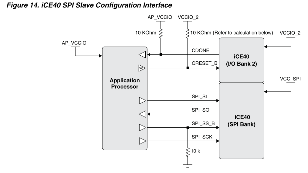
In the case of NandBug, the Application processor is, in fact, the FT2232H.
To generate the needed SPI and GPIO signals, the FT2232H is used in MPSSE Mode. Detailed documentation about this mode can be downloaded from here.
Host side Tools
The host tools are written in Python and have the following functions:
- Generating one of the four bitstreams detailed above. This is done using nMigen.
- Uploading these bitstreams to the FPGA using the SPI Slave Mode programming procedure. This is done thanks to pylibftdi.
- Communicating with the configured FPGA to receive data from the NAND Flash or orchestrate programming operations.
Three scripts are available.
NandBugDumper.py
./NandBugDumper.py -h
usage: NandBugDumper.py [-h] filename

Dump the nand flash content

positional arguments:
  filename    output filename

optional arguments:
  -h, --help  show this help message and exit
This script will:
- Generate the Dump bitstream and upload it to the FPGA
- Receive the NAND Flash data and write it to the output
filename
NandBugPatcher.py
./NandBugPatcher.py -h
usage: NandBugPatcher.py [-h] [--last-dump LAST_DUMP] filename

Patch the nand flash content

positional arguments:
  filename              input filename

optional arguments:
  -h, --help            show this help message and exit
  --last-dump LAST_DUMP
                        use this dump instead of reading the flash content
This script will:
- Generate the Dump bitstream and upload it to the FPGA.
- Receive the NAND Flash data and compare it to the content of
filename. - Generate a list of blocks to erase and pages to program. This step can optionally be skipped if a
LAST_DUMPfile is provided. - Generate the Erase Blocks bitstream & upload it to the FPGA.
- Send a list of blocks to erase to the FPGA.
- Generate the Program Pages bitstream & upload it to the FPGA.
- Send the pages addresses and data to the FPGA.
NandBugPassthrough.py
This script will simply generate the Passthrough bitstream and upload it to the FPGA.
Conclusion
What’s Working Well
Overall, I’m pleased with how NandBug is working. The NAND Flash dumping and programming features are reliable.
More importantly, the Google Home Mini can still boot without problems despite all the heavy surgery it received.
For reasons that will become clear in my second article, these functions have been stress-tested quite heavily, with more than a hundred dumping, programming and “booting” operations.
Apart from attempting to run my own code of the Google Home, I guess this solution could also be used to keep track of all firmware updates performed by Google. Indeed, it’s possible to let the device run normally for an extended period of time while dumping the entire flash content from time to time.
Limitations
One of the very early design goals of NandBug was to be able to monitor the data read and written by the Google Home to the NAND Flash in real time. Altering this data on-the-fly was also an option. It could possibly have been useful to find interesting TOCTOU bugs in the secure boot implementation.
However, The NAND Flash signals are going too fast for achieving this with a simple ICE40 FPGA. This may have been possible with a more advance component.
This feature can somehow work a bit at the very beginning of the Google Home boot sequence, though. At this early point, the clock of the NAND Flash peripheral is reduced to a couple of hundreds of kHz.
Firmware Image Surgery
Making sense of the NAND Flash Dump
Thanks to NandBug, it’s now possible to easily dump the entire content of the NAND Flash. However, before even thinking of patching the firmware, making full sense of this dump is needed.
The first thing to note is that the way the data is written to a NAND Flash is somewhat special. A NAND Flash is composed of several pages. Each page contains data and a special section called OOB, the out-of-bound section.
The OOB section of each page is usually used to store Error Correction Code or ECC. This is needed because of how imperfect NAND Flash technology is. Bit flips are very common with these memories, and ECC are an efficient way to address the issue.
In our case, reading the datasheet of the NAND Flash used by the Google Home, the TC58NVG1S3HBAI6 gives the following details about the internal memory organization.
The TC58NVG1S3HBAI6 is a single 3.3V 2 Gbit (2,281,701,376 bits) NAND Electrically Erasable and Programmable Read-Only Memory (NAND E²PROM) organized as (2048 + 128) bytes x 64 pages x 2048 blocks.
So, for us, each page is 2716 bytes, with 128 bytes used as OOB.
Given this information, a graphical representation of the binary dumped data can quickly help check whether the OOB section is likely to be used for storing ECC or not.
Such a representation is given below. The width of the image is fixed to 2176 pixels, matching the size of a page. Hence, each line of the image corresponds to a single page. A red line is placed at 2048 pixels. It separates the main data from the OOB section.
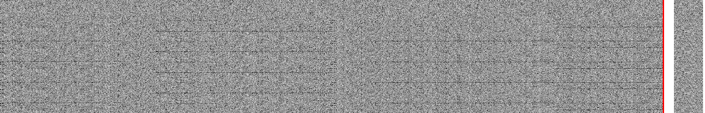
It appears that for each page, the OOB section is filled with a 90 bytes chunk of data.
This data looks high entropy, seemingly random. Further, for two identical “data” pages, the corresponding OOB area will be the same as well.

These visualizations combined with the datasheet can lead to the following conclusion:
- For each page, the data area is 2048 bytes
- The OOB area is 128 bytes.
- Each page is very likely using an ECC placed in the OOB area. The length of this ECC is 90 bytes.
Breaking the ECC code
We now know where the ECC information is written inside the memory dump. Now, it’s important to guess the algorithm used to generate this data. Indeed:
- It’s needed to correct the dump and to go further with unpacking the firmware files. As I explained before, NAND Flash memories are unreliable and the probability some bits are flipped is high.
- My goal is not only to read, but also to alter the NAND Flash data to achieve code execution. Hence, the ECC of all modified pages must be computed. Otherwise, the Google Home Processor will simply discard all the modified pages.
In order to have a better understanding of how the code was calculated, I started to take a look at the released bootloader and Linux Kernel code available from the shared files I talked about in the first section of the article.
A glance at the bootloader/berlin_tools/bootloader/nand_ctrl/mv_nand.c file is enough to understand the ECC is calculated by the hardware of the main SoC itself. The NAND Flash hardware peripheral of the processor is fully responsible for computing it. The only hint the source can give is that the ECC algorithm in use is very likely BCH.
However, this information alone isn’t enough to compute the ECC in the same way with the hardware. At least, the BCH polynomial used is also needed.
Going one step further, it’s possible to grep for interesting strings in the binary dump.
$ strings dump.bin.fixed | grep ecc
[...]
NAND ecc capability:              48
[...]
This could mean the BCH polynomial is selected in such a way that 48 flipped bits can be corrected for each page.
Playing with the bchlib Python library somewhat confirmed this hypothesis. The length of the ECC data we measured thanks to the graphical visualization could match a BCH-48 algorithm.
import bchlib

data = b"\xAA" * 0x820

bch = bchlib.BCH(0x8003, 48)
ecc = bch.encode(data)

print(f"len(ecc) = {len(ecc)}")
$ python test_ecc.py
len(ecc) = 90
However, with these BCH parameters, while the size of the codeword was matching what was observed in the real hardware, the computed ECC data was wrong. This could mean several things:
- BCH wasn’t actually used.
- The selected polynomial was wrong.
- Another transformation was applied to the data before or after BCH encoding.
From here, the most frustrating part of this entire study began. I spent hours trying to figure it out. I truly thought it was the end of it and almost gave up. But I finally found the trick!
The ECC code is actually computed in the following way:
- Swap the nibbles of each of the 2080 first bytes of the page.
- Compute a BCH code with
p=0x8003andstrength=48. - Swap another time the nibbles of the computed BCH code.
I guess this nibbles swapping weirdness is caused by the way the low-level hardware BCH engine is actually working.
With this problem out of the way, fixing the binary dump became possible. A couple of hundreds of bit-flips were corrected this way.
It was now time to actually take a look at the content of the NAND Flash dump.
Unpacking the Firmware Image
The NAND Flash Layout
Using strings and grep against the firmware dump can quickly reveal interesting bits of information.
For instance, the entire NAND flash layout (i.e., the partitions) can be revealed in the following way.
$ strings dump.bin.fixed | grep mtdparts
[...]
init=/init console= mtdblock.ro_fspart=rootfs nooverlayfs flash_ts.dev_id=0 flash_ts.size=524288 flash_ts.erasesize=131072 flash_ts.writesize=2048 androidboot.bootloader=8ac32c4-dirty nandboot.src_block_num=0x00002d0901010101 sd8887.cal_data_cfg=mrvl/WlanCalData_sd8887-b1.conf sd8887.fw_name=mrvl/sd8887_wlan_a2.bin sd8887.auto_ds=2 sd8887.mac_addr=[REDACTED] sd8887.txpwrlimit_cfg=mrvl/txpwr sd8887.cfg80211_drcs=0 sd8887.ps_mode=2 sd8887.uap_oper_ctrl=0x20001 bt8xxx.fw_name=mrvl/sd8887_bt_a2.bin bt8xxx.bt_fw_serial=0 warm_boot=1 prng_data=8340fd293316011b56322f500ff7f90b19366c070cd98925dbf898eb4008e0d6db1d3478121b7f25f92cf822750073c0a4a84989f54abb98f0079e583eb6b236 root=/dev/mtdblock:rootfs mtdparts=mv_nand:128K(block0)ro,1M(prebootloader)ro,2304K(TZ)ro,2304K(TZ-B)ro,640K(postbootloader)ro,640K(postbootloader-B)ro,4608K(kernel)ro,90M(rootfs)ro,149248K(cache),7M(recovery),1M(factory_store)ro,512K(fts)ro,384K(bbt)ro androidboot.hardware=joplin-b4 androidboot.mode=normal
[...]
Here, the Linux Kernel command line contains the mtdparts configuration variable. This leaks both the names and sizes of all flash partitions.
| Index | Partition | Size |
|---|---|---|
/dev/mtd0 | block0 | 128K |
/dev/mtd1 | prebootloader | 1M |
/dev/mtd2 | TZ | 2304K |
/dev/mtd3 | TZ-B | 2304K |
/dev/mtd4 | postbootloader | 640K |
/dev/mtd5 | postbootloader-B | 640K |
/dev/mtd6 | kernel | 4608K |
/dev/mtd7 | rootfs | 90M |
/dev/mtd8 | cache | 149248K |
/dev/mtd9 | recovery | 7M |
/dev/mtd10 | factory_store | 1M |
/dev/mtd11 | fts | 512K |
/dev/mtd12 | bbt | 384K |
Extracting all these partitions to individual files and removing the OOB data if needed was now just a matter of writing a small script.
Let’s now take a brief look at the content of these sections.
The Kernel Image
The partition untitled kernel does contain an android bootimg.
$ binwalk kernel.bin

DECIMAL       HEXADECIMAL     DESCRIPTION
--------------------------------------------------------------------------------
332           0x14C           Android bootimg, kernel size: 2443899 bytes, kernel addr: 0x5008000, ramdisk size: 1738760 bytes, ramdisk addr: 0x6000000, product name: ""
2380          0x94C           Linux kernel ARM boot executable zImage (little-endian)
4608          0x1200          device tree image (dtb)
27333         0x6AC5          xz compressed data
2437484       0x25316C        device tree image (dtb)
2437801       0x2532A9        Unix path: /home/jszhang/_install,vers=3 ip=::::bg2-cdp::dhcp macaddr=00:78:73:AB:38:CF mtdparts=mv_nand:1M(block0)ro,8M(bootloader),7M(fts
2447692       0x25594C        xz compressed data
The Linux Kernel version and compilation timestamp can be extracted from strings present in the binary data.
Linux version 3.8.13+ (user@host) (gcc version 4.9.x 20150123 (prerelease) (4.9.2_cos_gg_4.9.2-r203-ac6128e0a17a52f011797f33ac3e7d6273a9368d_4.9.2-r203) ) #0 SMP PREEMPT Fri Jun 7 12:32:44 2019 -0700 (78e8f601)
The Kernel seems to be based on a rather old version, 3.8.13. Given the compilation timestamp, the 7th of June, it’s possible to find the corresponding sources among Google’s shared files.
An initramfs filesystem can also be extracted. It contains a long initialization script, init.rc.
This script is basically responsible for mounting partitions and launching various services.
Please note the Kernel version, sources, initramfs and init.rc file will be useful in the second part of this series of articles.
The “rootfs” Partition
The simple file utility can be used against this image to reveal it’s, in fact, a Squashfs filesystem.
$ file rootfs.bin

rootfs.bin: Squashfs filesystem, little endian, version 1024.0, compressed, -2460550875131674624 bytes, 755302400 inodes, blocksize: 512 bytes, created: Thu Jan  1 00:00:00 1970
Extracting files from this image is just a matter of running the unsquashfs command.
Rebuilding the image, if ever needed, can be achieved thanks to mksquashfs.
All the ELF executables, scripts, and libraries ever run by the Google Home Mini are contained in this partition.
The “cache” & “factory_store” Partition
Reading through the init.rc script of the initramfs, it appears these two partitions are YAFFS2 partitions.
mount yaffs2 mtd@cache /cache noexec rw nosuid nodev noatime
# [...]
mount yaffs2 mtd@factory_store /factory_setting ro nosuid nodev noatime
# [...]
In order to mount and eventually alter the content of these partitions, I choose to use the same YAFFS2 driver that can be found on Google’s shared files.
To achieve this result, I simply compiled the entire Kernel sources provided by Google. I built this Kernel for the vexpress-a9 machine, an ARM Cortex-A9 machine supported by the system emulation tool qemu.
On this system, a NAND Flash can be entirely simulated thanks to the kernel NAND Simulator nandsim.
Here, I’m voluntary giving a very brief overview of this setup. Indeed, I’m planning to publish a way more detailed description of it in the second part of this study.
Once mounted, the cache reveals it’s mostly used to store user data and configuration files. For instance, a wpa_supplicant.conf (wpa_supplicant main configuration file) file storing Wi-Fi credentials exists.
The factory_store partition hosts various calibration files (calibrated values for LEDs brightness, …), serial numbers, but also client certificates used when the Google Home is communicating with Google’s servers.
The Other Partitions
Finally, here is a quick overview of the remaining partitions. Contrary to the others, I haven’t done a very in-depth study on them.
block0: This contains information needed by the BootROM of the main Marvell processor. This data is used to configure the DDR memory, the ECC algorithm used to read and write the NAND Flash, …prebootloader: I haven’t studied this section of the NAND Flash. It’s likely responsible for some low-level hardware initialization.TZandTZ-B: High-entropy data (likely ciphered), given the name, it may be linked to ARM TrustZone?postbootloaderandpostbootloader-B: This bootloader loads and verifies the Kernel image. The source code for this piece of code is part of the files Google shared. The Chromecast vulnerability I talked about at the very beginning of this article was located in this very binary.recovery: Another android bootimg. The scripts contained in the initramfs perform a factory reset of the Google Home Mini device.fts: According to the Linux source code, it is a Flash-based transactional key-value store. It contains various configuration variables.bbt: bbt stands for Bab Block Table. This contains indexes of all the bad blocks of the NAND Flash. This area is read at boot time, so the system knows which blocks of the NAND not to use.
Achieving Code Execution
First Naive Attempts
So, given the available content of the NAND Flash, how to proceed to run custom on the Google Home Mini?
At first sight, the content of several partitions can be discarded:
- The
TZandTZ-Bare ciphered and could even be linked to the ARM TrustZone. That’s way too big of a challenge for now. - We know the bootloader and
kernelpartitions are part of the chain of trust. They are cryptographically verified. Unsurprisingly, because they are probably the most carefully written parts, I haven’t been able to find any way to skip the secure boot from this side. - The
ftsandbbtare not filled with executable data. - Both the
cacheandfactory_storepartitions are mounted with thenoexecflag.
What’s left is the rootfs partition. Or at least that’s what I naively thought during my first attempts.
After having:
- Backdoored some binaries of the
rootfspartition - Rebuilt the Squasfs image with
mksquashfs - Recreated a NAND Flash image with carefully computed ECC words stored in the OOB section
- Flashed the NAND with NandBug
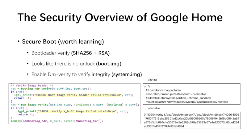
I sadly realized the Google Home Mini was not booting anymore. I quickly understood how naive I was by reading the init.rc script from the Kernel initramfs.
# [...]
# Load device mapper table
exec /sbin/dmsetup create system -r /dmtable
# [...]
The content of the /dmtable file is as follows.
0 143216 verity 1 /dev/block/mtdblock7 /dev/block/mtdblock7 4096 4096 17902 17902 sha256 0dbf4db75469a183a7efaba48a5b92f5e701864c945155bf578484e649840bfb 4558c8018b94ab29cdbe9ffa334a881eb6981be7b99bf81566c1f5f6c390d2d9
The rootfs is actually verified by dm-verity.
It shouldn’t actually have been a real surprise to me, as it was clearly stated in the DEFCON slides I linked to at the very beginning of the article.
A Dead-End?
So, with the rootfs out of the way, what’s left?
While all the executable data is apparently verified, having a total control on all the NAND Flash data does open a rather large attack surface.
Can a bug somewhere in this newly available attack surface be exploited? We’ll discover this in the second blog post dedicated to the Google Home Mini.
Spoiler alert: yes, there is an exploitable bug. That’s why, there is a second part.
Conclusion
I introduced NandBug. This system can be used to easily dump and alter the NAND Flash of the Google Home Mini, essentially making it In-System Programmable.
This method is useful for multiple things. For instance, keeping track of the Google Home Mini firmware releases becomes relatively easy. Further, attempting to run arbitrary code on the device from the NAND Flash becomes possible.
Apart from being an interesting challenge, running arbitrary code on the Google Home could be interesting for several reasons. Indeed, because the processor of the Google Home Mini comes without any public datasheet, arbitrary code execution can lead to a way better understanding of the system. It also makes further research easier. Finally, it may be a mandatory step if one’s goal is to dump the very low-level bootROM code of the main processor.
However, even considering this easy access to the entire NAND Flash data, an extended secure boot implementation makes executing arbitrary code using naive methods impossible. But, as the second part of this article will demonstrate, it remains possible.
Part 2 is available here.