Laser Fault Injection on a Budget: RP2350 Edition
Posted on Tue 14 January 2025 in Projects
Introduction
In August 2024, Raspberry Pi introduced the RP2350 microcontroller. This part iterates over the RP2040 and comes with numerous new features. These include security-related capabilities, such as a Secure Boot implementation.
A couple of days after this announcement, during DEFCON 2024, an interesting challenge targeted at these new features was launched: the RP2350 Hacking Challenge.
After some work and the development of a fully custom “Laser Fault Injection Platform”, I managed to beat this challenge and submitted my findings to Raspberry Pi.
This article will provide technical details about this custom platform, including manufacturing files for those interested in building their own. Additionally, I will explain how injecting a single laser-induced fault can bypass the Secure Boot feature of the RP2350.
Warning
The “Laser Fault Injection Platform” introduced in this article makes use of an infrared high-power laser source. Such a component can be hazardous; be careful if you attempt to reproduce this work.
Hacking Challenge & RP2350 Security Features
Objectives of the Challenge
The target of this challenge is a Pico 2 board, which hosts a RP2350 microcontroller. It must be configured according to the instructions provided in the challenge’s GitHub repository.
Following the instructions from the repository will:
- Write “secret” data into one of the OTP areas of the
RP2350. - Configure and enable the Secure Boot feature, locking the chip as much as possible. This includes disabling debug interfaces (SWD) and enabling various security features, such as glitch detectors.
- Flash a signed firmware that primarily restricts even more access to the OTP area where the secret is stored.
The goal of the challenge is to find a way to recover the secret data, potentially bypassing the Secure Boot feature in the process.
Security Features
The Secure Boot feature is enforced by code contained in the Boot ROM of the RP2350. This code is hardened in several ways, going beyond software methods; the Boot ROM leverages hardware-specific features.
These features are primarily related to an innovative component called the “Redundancy Co-Processor.” Quoting the RP2350 Datasheet:
The redundancy coprocessor (RCP) is used in the RP2350 bootrom to provide hardware-assisted mitigation against fault injection and return-oriented programming attacks. This includes the following instructions:
- generate and validate stack canary values based on a per-boot random seed
- assert that certain points in the program are executed in the correct order without missing steps
- validate booleans stored as one of two valid bit patterns in a 32-bit word
- validate 32-bit integers stored redundantly in two words with an XOR parity mask
- halt the processor upon reaching a software-detected panic condition
[…]
Each core’s RCP has a 64-bit seed value (Section 3.6.3.1). The RCP uses this value to generate stack canary values and to add short pseudorandom delays to RCP instructions.
Additionally, the RP2350 is capable of detecting fault injection attempts using glitch detectors. These configurable circuits respond to voltage or electromagnetic fault-injection attempts and reset the system. For this challenge, these detectors are set to their maximum sensitivity level.
Article Overview
Below is a brief, high-level summary of the article’s content.
Why choosing Laser Fault Injection
Considering that the Boot ROM of the RP2350 has been audited before the opening of the challenge, I did not attempt to find logic bugs in it and quickly considered a hardware attack, such as a fault injection attack.
However, online comments tend to show that the glitch detector system implemented in the RP2350 was rather efficient in mitigating simple voltage fault injection attacks.
Hence, I quickly decided to tackle the challenge with laser fault injection, assuming that focusing a laser beam away from the glitch detector circuits could allow for injecting faults without triggering them.
Now, the thing is, while I did have some experience with “classic” voltage fault injection attacks, I knew nothing about laser fault injections.
This challenge was then used as an opportunity to build a fully custom, cheap laser fault injection platform.
Note that while traditionally known to be expensive to implement, several “cheap” platforms aimed at injecting faults with a laser have emerged over the past few months:
- Laser Fault Injection for The Masses is repurposing laser engraving hardware.
- The “RayV-Lite” from NetSPI.
However, at the time of writing, very few publicly available technical details are available regarding this project.
Note
My mistake, after some research, I actually managed to find this presentation of the “RayV-Lite” introduced at Blackhat 2024. Their project presents various similarities with my “Laser Fault Injection Platform”, but also interesting differences. I’ll highlight some of these differences in this article and encourage you to check out their work.
August 2025 update: Even more material is now publicly available! This includes an article on NetSPI’s website.
Sample Preparation
The idea being LFI is reasonably simple. A focused laser beam is directed at the silicon die of the target component. Transistors are sensitive to photoelectric effects, meaning the emitted light can be enough to induce temporary faults or malfunctions. When precisely timed, these faults could be leveraged to bypass security features.
A major downside of such an attack compared to voltage or clock glitching is that the silicon die of the target has to be exposed. Of course, the circuit must still be able to operate normally after the die has been exposed.
Accessing the silicon can either be attempted from the top, or the bottom side of the packaged chip.
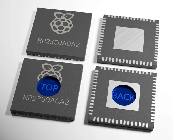
I chose to expose performed from the backside of the die. This choice has been made for two reasons:
- Accessing the backside can be achieved with cheap mechanical tools. However, exposing the top of the die would have required chemicals I would rather not deal with, such as concentrated nitric acid.
- Based on images available online, it seems the top of the die is fully covered by a metal layer, likely complicating fault injection.
The process I developed to expose the backside of the silicon die is detailed in the relevant sections of this article.
Die Imaging & Laser Focusing
LFI requires targeting with a focused laser beam relatively precise areas of the die. A custom, cheap Laser Fault Injection platform has been designed for this purpose.
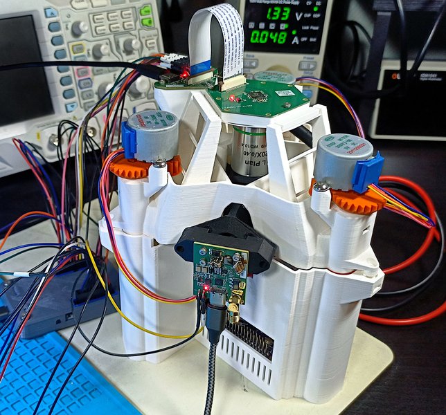
Because the design of this platform is very budget oriented, corners had to be cut in multiple paces, resulting in various limitations. These limitations, alongside various technical details and working principles, are detailed in the corresponding sections of this article.
To enable others to reproduce my results, I will also be sharing the relevant manufacturing files and source code.
Fault Injection & Secure Boot Bypass
Being able to inject faults is just the first step in attacking the RP2350. As previously mentioned, the glitch detectors are not the only security feature that Raspberry Pi developed to protect the system.
It is also necessary to identify a weakness in the Boot ROM of the component, where the Secure Boot feature is implemented. The specific sequence of instructions I targeted will be discussed in the relevant sections of this article.
Sample Preparation
This section describes the initial steps required to execute the attack. The backside of the die of the target RP2350 must be carefully exposed, ensuring that the chip’s functionality remains intact.
Die Exposure
The target RP2350 first has to be desoldered from the Pico 2 board. This can be achieved with a simple hot air reflow station.
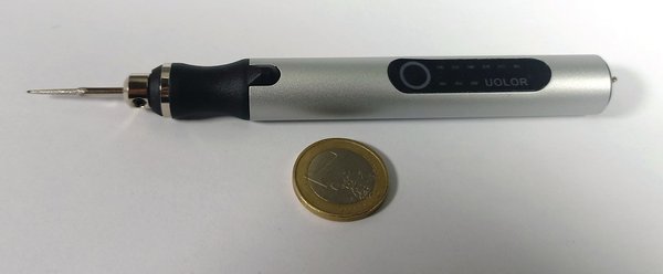
Next, a cheap (€30) dremel-like tool, advertised as an “Engraving Tool” (Amazon Part Number: UKH062_FR), has been used to carefully remove material around the ground pad.
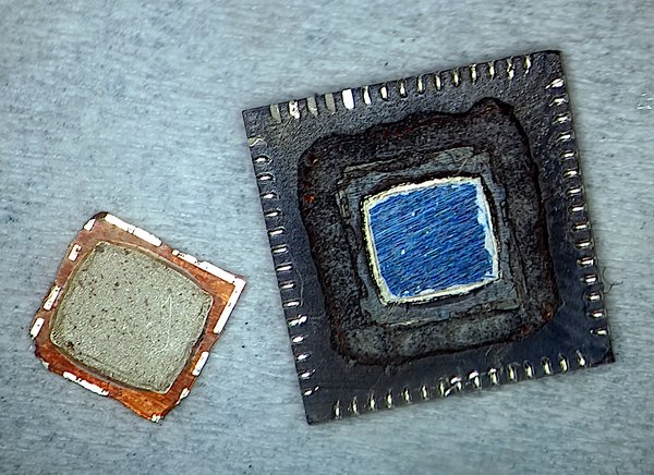
After enough material has been removed, the metallic ground pad can be taken off, exposing a layer of what looks like silver (heat-conductive?) paste. This paste can easily be scratched out, revealing the backside of the die.
Main Carrier Board
The prepared sample can then be soldered on a custom PCB, designed to integrate with the Laser Fault Injection Platform.
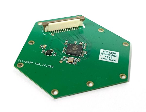
A hole in the middle exposes the backside of the RP2350 die.
The board doesn’t include anything more, apart from a small LDO used to power the core. Power and control signals are routed away to an FFC connector.
        flowchart LR
            B{{FFC Connector}} <-->|UART| A(RP2350)
            A <-->|SWD| B
            A <-->|USB| B
            A <-->|QSPI| B
            A <-->|Control Signals| B
            B .->|3V3| A
            B .->|3V3| C((LDO))
            C .->|1V1|A
This PCB can be hand-assembled, and the total unit BOM cost for small quantities is estimated at less than €10.
![]()
Interactive 3D Render & Design Files
I/O Board
The Main Carrier Board detailed above connects to the I/O Board through a FFC cable.
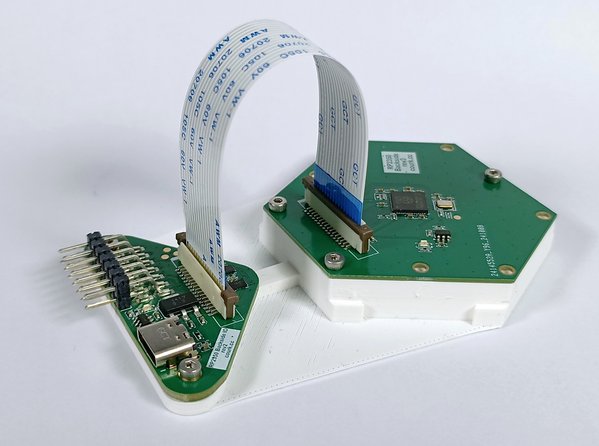
The assembly of these two boards is designed to integrate with the Laser Fault Injection Platform.
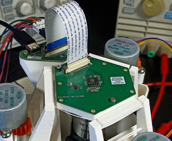
The I/O Board breaks out the various control signals over:
- A USB connector
- Pin headers that are connected to a FPGA board, later used to implement the attack’s logic
- A few test points used for SWD debugging (seldom used, especially considering SWD needs to be disabled for this challenge)
        flowchart TB
            A((LDO)) .->|3V3| B((Power Switch))
            C{{USB Connector}} .->|5V| A
            C <-->|USB| D{{FFC Connector}}
            B .->|3V3| D
            E{{Pin Headers}} -->|Enable| B
            D <-->|Control Signals| E
            D <-->|QSPI| E
            D <-->|UART| E
            D <-->|SWD| F(Test Points)
            D <-->|QSPI| G(QSPI Flash #0)
            D <-->|QSPI| H(QSPI Flash #1)
Additionally, two QSPI flashes are mounted to the board. The “active” flash, i.e. the one connected to the ~CS line of the RP2350, can be selected from the FPGA. This means the “active” flash can be swapped between each request from the RP2350 to the external memory.
This feature, detailed in the following diagram, is instrumental for the attack described in this article.
        flowchart LR
            A(RP2350) -->|CS| B(FPGA)
            B -->|CS#0| C(QSPI Flash #0)
            B -->|CS#1| D(QSPI Flash #1)
Here again, the board can be hand-assembled. The total unit BOM cost for small quantities is estimated to be less than €15.
![]()
Interactive 3D Render & Design Files
Ground Connection Repair
Note
August 2025 update: The method detailed here is overcomplicated. See Laser Fault Injection on a Budget: DEFCON 33 Showcase for a simpler method.
An obvious issue with removing the ground pad to access the die is that the only ground connection to the integrated circuit is destroyed.
The RP2350 has a PGND pin connected to its internal DC/DC converter, but it doesn’t seem to have a low-impedance internal connection to ground. Instead, a method to restore a sufficient ground connection has been implemented.
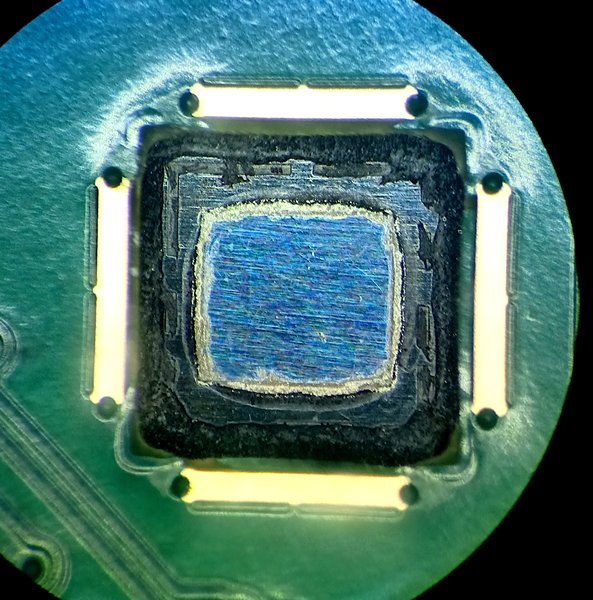
It’s a bit challenging to see, but specks of exposed copper (or gold?), as well as “holes” where severed bond wires likely passed, are visible. Slightly scratching these areas can sometimes reveal more conductive material.
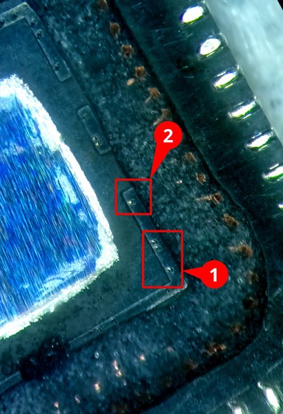
Magnified views of areas 1 and 2 are shown below.
Note
Note that these magnified images have been captured thanks to the imaging capabilities of the Laser Fault Injection Platform. This results in unusual colors, as the camera sensor of the platform lacks an IR filter.
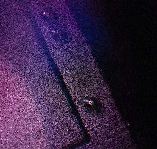
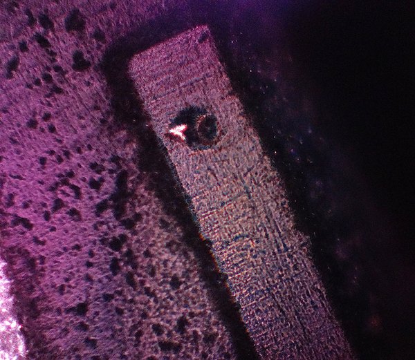
Applying conductive epoxy between these small exposed metal bits and purposefully arranged copper pads located on the Carrier Board was, thankfully, enough to restore a sufficient ground connection.
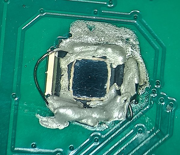
The reference for the product I used is MG CHEMICALS 9410. It’s a one-part, temperature-activated epoxy. I used a hot air station at for about 10 minutes to cure it.
Limitations
This process is, of course, a bit risky. While I’ve gotten better at it after a few attempts, I don’t think I can claim a 100% success rate.
Additionally, the ground connection restored thanks to the conductive epoxy is far from perfect. For instance, I’m usually not able to run such a modified RP2350 at high clock speeds, as it results in higher current being drawn.
Finally, I found that some I/O pads can sometimes stop working, or are facing signal integrity issues. I’m not sure all ground bond wires are internally connected on the die; I may not restore a good enough connection for all of them.
However, the target of the attack is the Boot ROM. The hardware is configured very conservatively by this ROM: clock speeds are low, etc. In this context, the “ground connection repair” method appears to be good enough.
To overcome these issues, it may be possible to mill only the very center of the ground pad, exposing the die while keeping the bond wires intact. This would likely require access to a CNC milling machine and fine bits, which I currently do not have.
Laser Fault Injection Platform
Platform Overview
As explained above, a custom fault injection platform has been designed for this project. While this hardware setup may not compete with more professional systems in terms of repeatability, it is likely an order of magnitude cheaper.
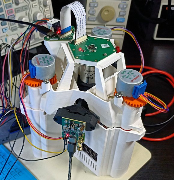
The platform can be divided into two subsystems, each of which will be detailed separately:
- A positioning stage, used to precisely displace the die of the target
RP2350for observation and laser focusing. - An optical subsystem, utilized for visualizing this die and focusing high-power laser pulses onto it.
Positioning Stage
The positioning stage is based on the OpenFlexure Delta Stage (McDermott et al., 2022). OpenFlexure projects are impressive, and I would not have achieved much without them. High-precision mechanical positioning is made possible with simple 3D printed parts and affordable stepper motors.
Note
The “RayV-Lite” system is also based on an OpenFlexure project, but not on the Delta Stage I selected here.
Minor modifications have been made to the official OpenFlexure Delta Stage:
- The base of the stage was raised to accommodate the custom optical subsystem.
- Heat-set threaded inserts have been added in various locations to support the custom electronics introduced in the previous sections of this article.
![]()
Interactive 3D Render & Design Files
Optical Subsystem
The optical subsystem is utilized for visualizing the die and focusing high-power laser pulses onto it. This subsystem is inspired from the reflection illumination subsystem from the OpenFlexure project. However, unlike the positioning stage, significant modifications have been implemented.
![]()
Interactive 3D Render & Design Files
The Necessity of Using Infrared Light
One of the downsides of attacking the die from its backside is that infrared light has to be used. Indeed, silicon is almost fully opaque to visible light, preventing both visualization and fault injection.
Instead, infrared light with a wavelength of is utilized. This wavelength is traditionally employed for backside fault injection and can also, as demonstrated in Infra-Red, In Situ (IRIS) Inspection of Silicon (bunnieHuang, 2023), be used for visualization of the die’s features.
Optical Components
The 3D render available below is extracted from the complete Laser Fault Injection Platform 3D Render. Only the components relevant to the imaging and laser focusing features are displayed and annotated.
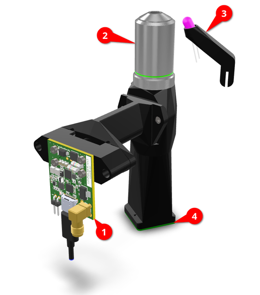
The following items are visible. Refer to the Optical Assembly page for exact part numbers or sourcing details.
- The Laser Driver Board - This custom PCB is used to drive a laser diode, emitting short but powerful pulses of light. This piece of hardware will be detailed later in this article.
- Objective Lens - This is an off-the-shelf microscope objective lens. I wanted an infinity-corrected one to make focusing the laser beam easier. Unfortunately, these are typically more costly than finite-corrected ones. I obtained one for about €90 from AliExpress.
- Oblique Illumination System - This is a simple LED, used for imaging the die. During my tests, I noticed that illuminating the sample from its side, with a rather narrow angle, resulted in the best image contrast.
- Imaging Camera - This is a Raspberry Pi Camera v2 “NoIR”. As it does not have an IR filter, it remains a bit sensitive to the wavelength of interest.
Removing even more objects, including the 3D-printed parts that are holding things together, the following new optical elements become visible.
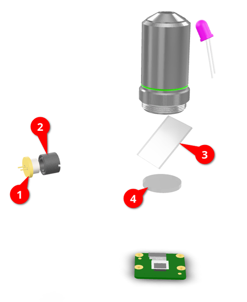
- Laser Diode - A laser diode. This tiny component was by far the most challenging part to source. I negotiated five pieces on Alibaba for about €300.
- Adjustable Collimating Lens - A screwable lens used to collimate the output of the laser diode. It can be purchased in bulk for a low price on AliExpress.
- Beam Splitter - This piece of glass is specially coated to reflect a fraction of the incoming light while transmitting the other part. Purchased for a reasonable price on AliExpress.
- Tube Lens - Once again, purchased for a reasonable price on AliExpress.
As explained, most of these components are off-the-shelf and have been sourced cheaply from Aliexpress. However, there is still a cost: these parts are often poorly specified or designed primarily for traditional microscopy applications, where only visible light is considered. As a result, I suspect that some infrared laser light is wasted and that the imaging may suffer from chromatic aberrations.
Optical Paths
Imaging
The path followed by the light to ensure the “Imaging” feature of the assembly is highlighted below.
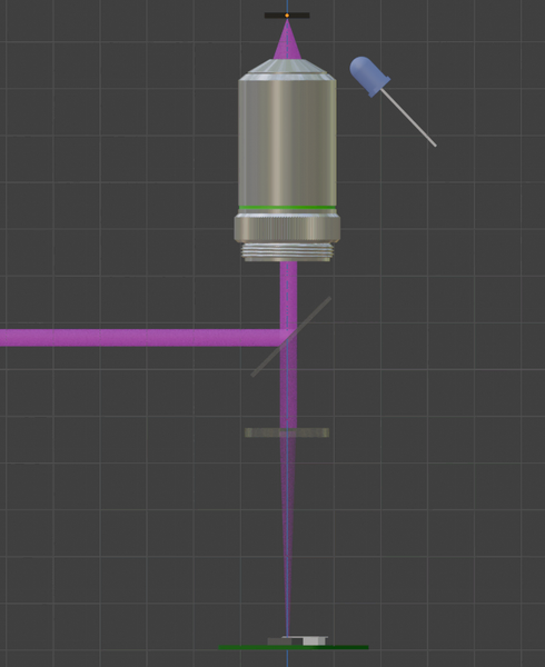
The sample is first illuminated by the Oblique Illumination LED. This wavelength passes through the silicon and reflects off the features of the die.
Note
While not as powerful as the laser, this LED still seems to interact with the circuit in some way.
In particular, I noticed that it was sometimes impossible for the system to boot when the die was illuminated by the LED. I suspect that analog circuits, which may be more sensitive than digital ones, are affected.
To avoid this problem, the LED is only turned on to image the die and align the laser beam. It is turned off during the attack process.
Next, this light passes through the infinity-corrected lens before being imaged back to the camera sensor thanks to the tube lens.
In between, the light goes through the beam splitter. A fraction of the light will be transmitted and continue in the same direction. The reflected fraction of the light is lost.
The selected beam splitter has the following properties:
- Reflection coefficient: 90%
- Transmission coefficient: 10%
This prioritizes the light coming from the laser beam, whose path is detailed below.
Laser Focusing
The path followed by the light to implement the “Laser Focusing” feature of the assembly is highlighted below.
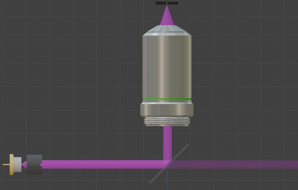
A pulse of light is emitted from the laser diode. This light is diverging and is collimated with the Adjustable Collimating Lens.
Most (90%) of the collimated light is reflected by the beam splitter and sent through the objective lens, where it is focused on the target sample.
Imaging Results
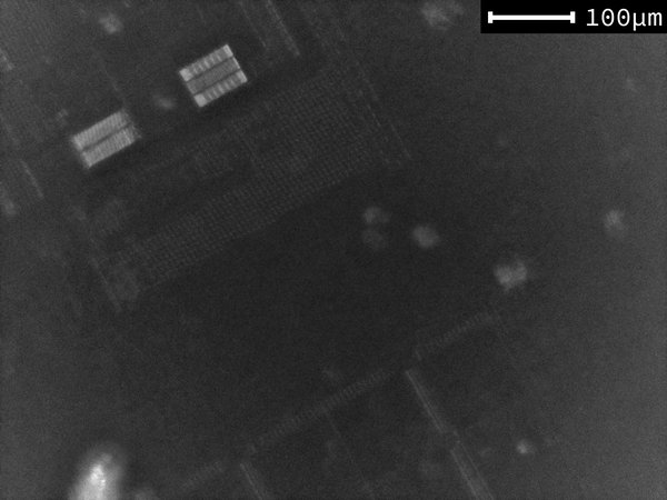
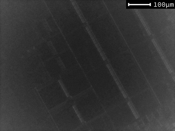
Below are a couple of slightly processed images of the die obtained from the setup.
Additionally, you will find a zoomable stitched view of the entire die.
Note
The quality of the stitching is obviously very poor; the processing tool I used struggles with the low-contrast images I provided.
For completeness, the following video demonstrates what is visible in real-time through the OpenFlexure web-based interface.
While these images may definitely not match the quality produced by a professional setup, they are sufficient to align a laser beam with specific features of the die.
The limiting factor may be the CMOS camera sensor, which is only marginally sensitive to . Unfortunately, cameras that are sensitive to these wavelengths tend to be quite expensive.
For a much better view of the backside of the die, check-out the one shared by @LennertWo.
Laser Focusing Results
The properties of the focused beam aren’t great, and the resulting spot is rather large and elliptical. That’s not ideal, as the goal is to achieve a high-power density to inject a fault.
An example of the resulting spot is available below. Note that here, the laser was pulsed at a reduced power to avoid blinding the camera sensor.
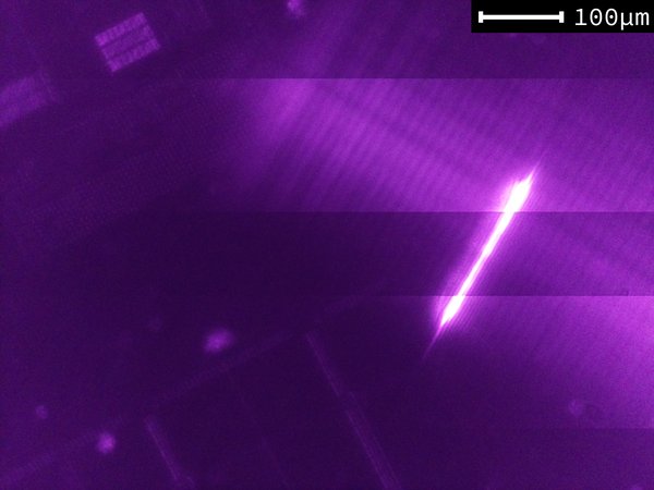
This problem has been mitigated by increasing the power supplied to the laser diode from the Laser Driver Board.
Multiple factors can explain the poor shape of the laser spot:
- The lenses I used are only specified for visible light.
- The focusing method is simple and possibly a bit naive; I’m no optical expert.
- Most importantly, the laser diode I used is a high-power one; the emitting element is large, and the light coming out of it is very diverging, with large differences between the fast and slow axes.
Laser Driving
Warning
This is where things can get dangerous. Although the custom board described here produces only very short pulses, working with a high-power laser can be hazardous, particularly when the emitted light falls outside the visible spectrum.
Be careful if you attempt to reproduce this work.
Laser fault injection requires short, high-power light pulses to be transmitted. A custom board has been designed for this purpose.
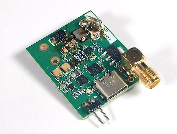
Most of the electronics are located on the top side of the board, with a laser diode installed on the bottom side.
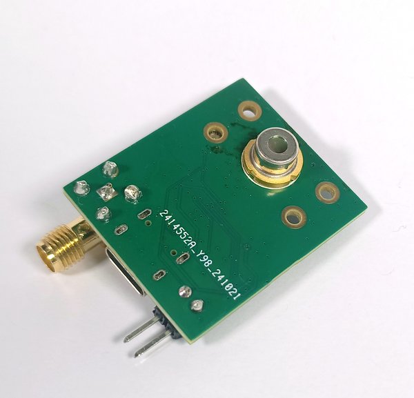
While designing such a board was not overly complicated, finding a suitable laser diode turned out to be more challenging.
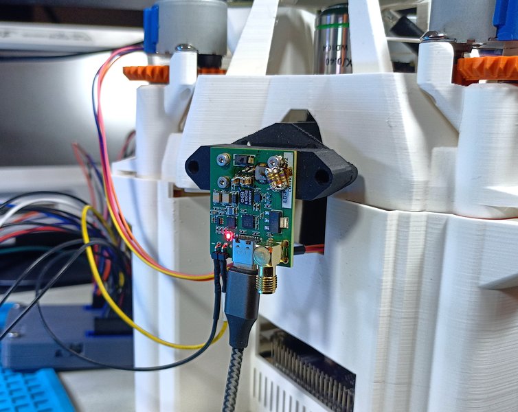
Note
As visible in the pictures of the boards, a section of the circuit has been reworked. This has been done to adjust the laser pulse parameters, as detailed below. The shared schematics have been updated to reflect this rework.
![]()
Interactive 3D Render & Design Files
Board Architecture
The architecture of the Laser Driver Board is outlined below.
        flowchart TB
            A{{USB Connector}} <--> B(USB to I2C Bridge)
            B -->|Configure| C(Digital Potentiometer)
            B -->|Trigger| E
            C .-> D(High Voltage Power Supply Circuit)
            D .-> E(Pulse Generator Circuit)
            E .-> F(Laser Diode)
            G{{Pin Header}} -->|Trigger| E
            F -->|Current Sense| H{{SMA Connector}}
The board is powered and configured from a USB port. The host computer connected to this port can be used to:
- Configure the output level of a high-voltage (up to ) power supply. This high supply is needed for the pulse generator circuit to operate.
- Manually send laser pulses.
However, because USB cannot be used for anything time-critical, laser pulses can also be generated from a simple pin header connector. This connector is interfaced with a FPGA board during the attack.
An SMA connector can be used to monitor the shape and intensity of the current pulses passing through the laser diode.
Pulse Generation Principle
A simplified schematic of the pulse generation circuit is outlined below.
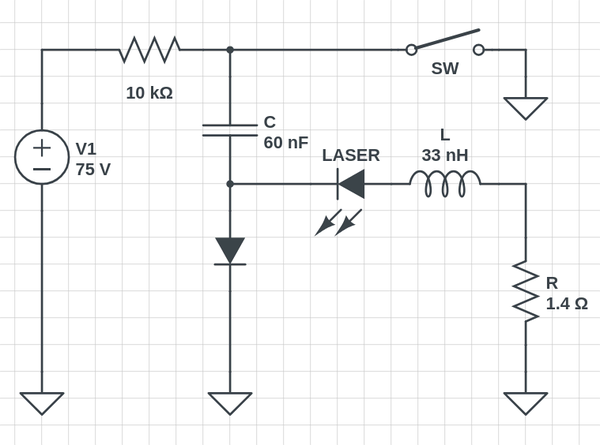
The capacitor C is first charged from the high-voltage power supply. To trigger a current pulse through the laser diode, the switching element SW is closed.
The current response is close to the one observed with a typical RLC circuit. The value of R is chosen to ensure the response of the circuit is critically damped.
C and L can be fine-tuned to change the duration of the pulse, while the high-voltage level can be used to set the peak current.
Unfortunately, this means that changing the pulse duration is only possible by soldering new components onto the board. I had to perform this rework several times, gradually increasing the peak current until faults were successfully injected.
The values that have been used to successfully exploit the RP2350 are:
Note that the selected resistor must be able to handle high current pulses. After having destroyed several parts, I ended up using Vishay’s CMB 0207 family.
The selected RLC values result in the following theoretical current pulses.
In practice, the pulses generated by the hardware are reasonably close to these theoretical curves.
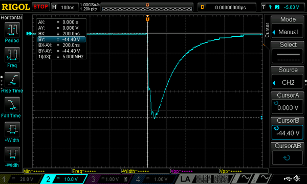
Unfortunately, in part because the optical components (lenses, beam splitter) I used are not specified for infrared light, I’m not sure how these current curves translate to the actual optical power received on the die surface.
Finally, note that the switching element SW is implemented with a fancy GaN FET. This choice was initially made to experiment with ultra-short pulses. However, it turns out that this wasn’t particularly useful. The BOM cost could be reduced by opting for a simpler MOSFET instead.
Despite this, the price of this BOM for small quantities does not exceed €30, excluding the cost of the laser diode.
Laser Diode Sourcing
Finding a suitable laser diode was challenging. It turns out high-power laser diodes are difficult to find and expensive!
After a few unsuccessful attempts (i.e. not enough power to inject a fault without damaging the diode first) with low-power parts (below ), I contacted a manufacturer on Alibaba and was able to order, for about €300, five pieces of a part rated for . The datasheet for this part is available here.
This datasheet clearly states that the maximum operating current is . Based on the current curves shared above, it’s very obvious the part is used well above its rating.
While I anticipated encountering catastrophic optical damage issues, even after several thousand pulses, I don’t think I have harmed these diodes yet! This might be due to the short duration of the current pulses.
This surprising result matches the observation of Continuous wave laser diodes enable fast optoacoustic imaging (Stylogiannis et al., 2018):
We investigated whether continuous wave (CW) laser diodes, which are available in visible and near-infrared regions, can be good optoacoustic light sources when overdriven with a peak current >40-fold higher than the CW absolute maximum.
Note
A major difference between my work and that of the team behind the “RayV-Lite” system is that they used a widely available laser diode marketed as a “green” one.
That’s a clever choice, as it seems that, because of the way green light is actually generated, such diodes typically emit a significant amount of power at . (Galang et al., 2010)
Fault Injection Results
Identification of Sensitive Areas
After developing the Laser Fault Injection Platform, it was time to actually attempt to inject faults into a RP2350.
I first began studying the effect of laser pulses on a dummy firmware, similar to the one proposed by Hextree.io in their RP2350 Security Playground Demo.
I slowly scanned various areas of the die, varying laser power, focus, and other parameters. However, I did not attempt to comprehensively characterize the behavior of the system over the entire die surface area for the following reasons:
- It’s a slow process; in the interest of time, I stopped as soon after I was able to disturb the ARM core execution flow without triggering the Glitch Detectors.
- I hit a couple of areas that resulted in a full crash of the system and high power consumption. Considering that preparing samples is a bit tedious, I would rather not damage parts this way.
The sensitive surfaces I exploited are roughly located within the area highlighted below. Because the positioning repeatability of the Laser Fault Injection Platform isn’t perfect, while attempting to exploit the chip, I typically moved the beam slowly around these locations.
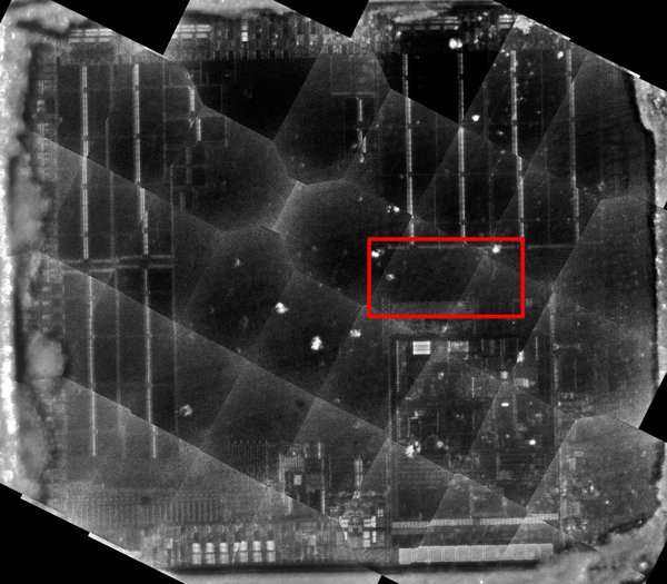
I found that depending on where the code is running from (SRAM, Flash, or ROM), or possibly based on the type of instructions being executed, it appears that slightly different locations had to be targeted to obtain interesting results.
Targeting for Secure Boot Bypass
The exact beam location used for the first Secure Boot bypass I achieved is displayed below. Here, the laser is pulsed at a low power to avoid blinding the camera.
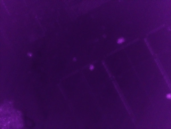
Secure Boot Feature Bypass
Constraints
Thanks to the Laser Fault Injection Platform, injecting faults without triggering the glitch detectors is now possible! However, this alone is not enough to bypass the Secure Boot feature implemented in the Boot ROM of the RP2350. Indeed, as highlighted earlier, the Boot ROM is hardened and uses various features to resist faults. Trivial methods, such as glitching a conditional branch choosing between a valid or invalid signature, aren’t directly possible.
Furthermore, when searching for a way to bypass the Secure Boot feature, the following constraints must be considered:
- With my custom hardware, I can only hope to inject a single fault at a time; complicated schemes with multiple glitches in a row aren’t possible. The limiting factor is the Laser Driver Board: the capacitor bank needs a bit of time to be recharged after each pulse.
- The laser pulse should be triggered following an observable external event, such as the activity of the QSPI bus.
- Random delays can be introduced by some instructions executed by the redundancy co-processor. Ideally, to target specific instructions, few to none of these special instructions should be executed between the trigger event and the fault injection.
Boot ROM Analysis Method
The source code of the Boot ROM of the RP2350 is publicly available. That’s really nice, and it makes high-level analysis of the Secure Boot way easier! Kudos to Raspberry Pi!
However, to study the possible impact of fault injections, I found it much easier to reflect directly against the actual ARM assembly code. Hence, after a quick read of the source code, I spent most of my time in Ghidra, looking at the content of the Boot ROM ELF file, also shared by Raspberry Pi.
In doing so, I managed to find a way to bypass the Secure Boot that addressed the previously listed constraints:
- Things could work out with a single instruction “skip” (though “skip” may be a misnomer, “mutation” is maybe a better word).
- The instruction to target closely follows an observable QSPI transfer.
- At worst, a single random delay co-processor instruction is executed between the trigger and the instruction to target.
High-Level Idea
Let’s consider the s_varm_crit_ram_trash_verify_block function. This function is at the core of the Secure Boot implementation. A very stripped-down version of its implementation is available below.
// Start computing a hash
sb_sha256_init(&sha);

// Load the data from the flash to the RAM
s_varm_crit_mem_copy_by_words((uint32_t *)to_storage_addr,
                              resolve_ram_or_absolute_flash_addr(
                                  from_storage_addr),
                              (size + 3u) & ~3u);

// Feed the hash engine with the data, obtained from RAM
uint32_t *src = resolve_ram_or_absolute_flash_addr(to_storage_addr);
sb_sha256_update_32(&sha, src, size & ~3u);

// Include block data (containing source address, dest address and size)
// to the SHA-256 hash
sb_sha256_update_32(&sha, block_data, parsed_block->hash_def_block_words_included * 4);

// Finalize the hash
sb_sha256_finish(&sha, signature_workspace->hash.bytes);

// Do the complicated & well protected signature validation
sig_matches_image_keyx = s_arm8_verify_signature_secp256k1(signature_workspace->sig_context_buffer,
                                                           &public_key[0],
                                                           &signature_workspace->hash,
                                                           &signature[0]);
This code implements a very usual signature verification scheme: the firmware to validate is reduced down to a hash, which is fed to the signature verification algorithm.
        flowchart TD
            A[(Firmware Data in Flash)] --> B("`Memory Copy
            _s_varm_crit_mem_copy_by_words_`")
            B --> C[(Firmware Data in RAM)]
            C --> D("`SHA-256
            _sb_sha256_update_32_`")
            D --> E("`ECDSA Signature Verification
            _s_arm8_verify_signature_secp256k1_`")
            F[[Public Key]] --> E
            E -->|Signature Valid| R(Execute Firmware Data from RAM)
            E -->|Signature Invalid| S(Failure)
The idea is to inject a fault after the call to s_varm_crit_mem_copy_by_words and before the call to sb_sha256_update_32. This could result in the SHA-256 hash being computed against different data than the one that was previously loaded into RAM.
        flowchart TD
            A[(Firmware Data in Flash)] --> B("`Memory Copy
            _s_varm_crit_mem_copy_by_words_`")
            B --> C[(Firmware Data in RAM)]
            C --x Z@{ shape: bolt }
            Z --> D("`SHA-256
            _sb_sha256_update_32_`")
            D --> E("`ECDSA Signature Verification
            _s_arm8_verify_signature_secp256k1_`")
            F[[Public Key]] --> E
            E -->|Signature Valid| R(Execute Firmware Data from RAM)
            E -->|Signature Invalid| S(Failure)
            X[(Unexpected Data)] --> Z
            style X fill:#f9f,stroke:#333
            style Z fill:#f9f,stroke:#333
If the “unexpected data” used to compute the SHA-256 hash can match the one corresponding to a valid firmware, the signature verification will succeed, no matter the data loaded into RAM.
Fault Injection Scenarios
This section explores the impact of possibly interesting faults against various instructions located between the call to s_varm_crit_mem_copy_by_words and the call to sb_sha256_update_32.
Scenario #1 - Single Instruction “Skip”
Note
“Skip” is possibly a misnomer. In practice, the targeted instruction here could be mutated. However, for this specific scenario, the exact result of the mutation doesn’t matter too much.
The C code listed above translates to the following assembly pieces.
s_varm_crit_mem_copy_by_words is first called.
00001d5c: 1a 00              movs          r2,r3
00001d5e: 20 00              movs          r0,r4
00001d60: 0d 93              str           r3,[sp,#local_24]
00001d62: 01 f0 82 fb        bl            varm_to_s_native_crit_mem_copy_by_words_impl
00001d66: 0d 9b              ldr           r3,[sp,#local_24]
00001d68: 43 ec 70 07        mcrr          p7,0x7,r0,r3,cr0
00001d6c: ac e7              b             LAB_00001cc8
The implementation of the function, listed below, increments R1 until the target size has been reached.
0000346c: 19 fe 3a c7        mrc2          p7,0x0,r12,cr9,cr10,0x1
00003470: 10 b5              push          {r4,lr}
00003472: 03 46              mov           r3,r0
00003474: 22 b1              cbz           r2,LAB_00003480
00003476: 1a 44              add           r2,r3
    LAB_00003478:
00003478: 10 c9              ldmia         r1!,{r4}
0000347a: 10 c0              stmia         r0!,{r4}
0000347c: 90 42              cmp           r0,r2
0000347e: fb d3              bcc           LAB_00003478
    LAB_00003480:
00003480: c0 1a              subs          r0,r0,r3
00003482: 09 fe 3a c7        mcr2          p7,0x0,r12,cr9,cr10,0x1
00003486: 10 bd              pop           {r4,pc}
Next, after the function returns, R1 is kept untouched until the call to sb_sha256_update_32.
00001d02: 32 00              movs          r2,r6 // size
00001d04: 21 00              movs          r1,r4 // src
00001d06: 0f a8              add           r0,sp,#0x3c // sha context
00001d08: 02 f0 49 fb        bl            sb_sha256_update_32
If the instruction at 0x00001d04 can be “skipped”, the following will in effect be executed:
r1 = resolve_ram_or_absolute_flash_addr(from_storage_addr) + size;
sb_sha256_update_32(&sha, r1, size);
The data referenced by R1 is located in the memory-mapped area corresponding to the flash data. This specific area performs uncached reads, meaning that data will be retrieved directly from the external QSPI bus. An attacker can manipulate this data.
This is where the “dual flash” feature embedded in the custom I/O Board becomes useful, as it simplifies the process of pushing arbitrary values over the bus. If necessary, two reads from the same address can yield different data.
Scenario #2 - Register Value Corruption
During my tests, I observed that injecting faults between s_varm_crit_mem_copy_by_words and sb_sha256_update_32 often resulted in data being pulled from the flash starting from offset 0.
I don’t have a clear explanation, such as a simple instruction skip, regarding why this happens.
It could, for instance, mean that when the following is executed:
00001d02: 32 00              movs          r2,r6 // size
00001d04: 21 00              movs          r1,r4 // src
00001d06: 0f a8              add           r0,sp,#0x3c // sha context
00001d08: 02 f0 49 fb        bl            sb_sha256_update_32
The value of R4 points to the beginning of the memory-mapped area corresponding to the flash data.
Anyway, this means that once again, the call to sb_sha256_update_32 can use data under the control of an attacker instead of the data already loaded into RAM.
Scenario #3 - Instruction Mutation
The instructions corresponding to s_varm_crit_mem_copy_by_words are available below.
0000346c: 19 fe 3a c7        mrc2          p7,0x0,r12,cr9,cr10,0x1
00003470: 10 b5              push          {r4,lr}
00003472: 03 46              mov           r3,r0
00003474: 22 b1              cbz           r2,LAB_00003480
00003476: 1a 44              add           r2,r3
    LAB_00003478:
00003478: 10 c9              ldmia         r1!,{r4}
0000347a: 10 c0              stmia         r0!,{r4}
0000347c: 90 42              cmp           r0,r2
0000347e: fb d3              bcc           LAB_00003478
    LAB_00003480:
00003480: c0 1a              subs          r0,r0,r3
00003482: 09 fe 3a c7        mcr2          p7,0x0,r12,cr9,cr10,0x1
00003486: 10 bd              pop           {r4,pc}
If a fault can be injected at 0x00003486, it’s possible for the pop {r4,pc} instruction to be altered, possibly resulting in the value of R4 not being restored.
Before pop {r4,pc}, R4 corresponds to the last word copied from the flash memory to RAM, a value under the control of the attacker. This value could, for instance, be set to an address contained in the memory-mapped flash area.
R4 is subsequently used when calling sb_sha256_update_32.
00001d02: 32 00              movs          r2,r6 // size
00001d04: 21 00              movs          r1,r4 // src
00001d06: 0f a8              add           r0,sp,#0x3c // sha context
00001d08: 02 f0 49 fb        bl            sb_sha256_update_32
Once again, sb_sha256_update_32 could be forced to run against data pulled from the QSPI bus.
Attack Process
Software Architecture
Various software components have been developed to implement the logic of the attack and control the electronics.
FPGA
To synchronize the laser pulse with the execution of the Boot ROM, the activity of the QSPI is monitored by the gateware of an FPGA Board connected to the I/O Board.
The choice of the FPGA platform isn’t super critical as the RP2350 is clocked at a conservatively low speed when the Boot ROM is running. I chose to use a Glasgow Interface Explorer tool.
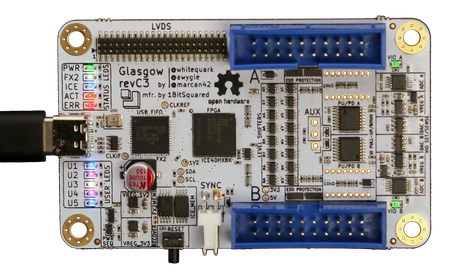
It embeds an iCE40 FPGA compatible with open source tools. Finally, it integrates well with Amaranth HDL, which I find more convenient to develop with than more common HDL languages like Verilog or VHDL.
The gateware written for this project is responsible for:
- Basic I/O Control:
- Turning the power supply of the target
RP2350on and off. - Controlling the
RUNandBOOTSELsignals.
- Turning the power supply of the target
- Trigger Timing: Monitoring the QSPI bus in real time.
- Attack Orchestration:
- Dynamically selecting the active QSPI Flash memory.
- Pulsing the laser.
Laser Driver Board
The Laser Driver Board communicates with the host computer through a USB-to-I2C bridge component.
No firmware running on the board needed to be written, and the host computer can be directly used to configure the high-voltage power supply for the laser diode pulser circuit.
Positioning Stage Control
The Positioning Stage is controlled by software running on a Raspberry Pi single-board computer.
The X, Y, and Z coordinates of the moving platform can be programmatically set using a web-based API.
In the context of this attack, this API is leveraged to slowly scan over the sensitive areas while pulsing the laser.
Laser Pulse Synchronization
The last QSPI read corresponding to the call of s_varm_crit_mem_copy_by_words can be detected with little uncertainty by the FPGA gateware. From this point, before calling sb_sha256_update_32, the following instructions are executed.
00003478: 10 c9              ldmia         r1!,{r4}
0000347a: 10 c0              stmia         r0!,{r4}
0000347c: 90 42              cmp           r0,r2
0000347e: fb d3              bcc           LAB_00003478
00003480: c0 1a              subs          r0,r0,r3
00003482: 09 fe 3a c7        mcr2          p7,0x0,r12,cr9,cr10,0x1
00003486: 10 bd              pop           {r4,pc}

00001d66: 0d 9b              ldr           r3,[sp,#local_24]
00001d68: 43 ec 70 07        mcrr          p7,0x7,r0,r3,cr0
00001d6c: ac e7              b             LAB_00001cc8

00001cc8: 0b 9b              ldr           r3,[sp,#local_2c]
00001cca: 00 2b              cmp           r3,#0x0
00001ccc: b3 d0              beq           LAB_00001c36
00001cce: 03 9b              ldr           r3,[sp,#local_4c]
00001cd0: 73 b1              cbz           r3,LAB_00001cf0
00001cf0: 23 0e              lsrs          r3,r4,#0x18
00001cf2: 10 2b              cmp           r3,#0x10
00001cf4: 02 d8              bhi           LAB_00001cfc

00001cfc: 03 23              movs          r3,#0x3
00001cfe: 3e 00              movs          r6,r7
00001d00: 9e 43              bics          r6,r3
00001d02: 32 00              movs          r2,r6
00001d04: 21 00              movs          r1,r4
00001d06: 0f a8              add           r0,sp,#0x3c
00001d08: 02 f0 49 fb        bl            sb_sha256_update_32
A redundancy co-processor instruction is executed at 0x00001d68, introducing a random delay of up to 127 system clock cycles. As a result, it becomes impractical to consistently time a laser pulse to target a specific instruction following 0x00001d68.
However, this instruction is the only one that introduces a random delay. The software designed for the attack allows for about 20 attempts per second, which is sufficient to inject interesting faults in a reasonable amount of time.
Flash Memory Organization
Before starting the attack, the two QSPI flashes of the I/O Board are organized as follows:
The first flash, whose content will be loaded to RAM, contains a copy of the valid, signed firmware, including a signature block, patched as follows:
- A small shellcode is written at the reset handler offset. This shellcode is designed to jump to arbitrary firmware located further in the flash memory at address
XIP_BASE + 0x10000.XIP_BASEcorresponds to the beginning of the memory-mapped flash data, while0x10000is an arbitrary offset. - The last word of the data loaded to RAM is set to
XIP_NOCACHE_NOALLOC_NOTRANSLATE_BASE + 0x7000.0x7000is an arbitrary offset that will be used later, whileXIP_NOCACHE_NOALLOC_NOTRANSLATE_BASEalso returns flash data.
The second flash, whose content is expected to be read after a fault has been injected, contains three copies of the unmodified firmware. Computing the SHA-256 hash against one of these images will result in a valid hash. The copies, ensuring all the fault injection scenarios that have previously been outlined, are located at:
- Flash offset
0x0, to support the Scenario #2. - The offset corresponding to the size of the data copied to RAM, to support the Scenario #1.
- Flash offset
0x7000, to support the Scenario #3.
Finally, an arbitrary firmware is copied at offset 0x10000. This firmware will run if the shellcode, previously loaded to RAM, is executed.
Attack Loop
During the attack, the following process is repeated in a loop.
- The first flash is selected.
- The
RP2350is powered on. - QSPI bus reads are monitored until the last byte corresponding to the call to
s_varm_crit_mem_copy_by_wordshas been read. - The second flash is selected.
- After an arbitrary delay, the laser is pulsed.
- QSPI bus reads are monitored again to verify if the data pulled from the flash corresponds to a successful bypass.
- In case of failure, the
RP2350is powered off, and a new attempt will be made.
        flowchart TD
            A[Select First Flash] --> B[Power On RP2350]
            B --> C[Monitor QSPI Reads]
            C --> D[Select Second Flash]
            D --> E[Arbitrary Delay]
            E --> F[Pulse Laser]
            F --> G[Monitor QSPI Reads]
            G -->|Failure| H[Power Off RP2350]
            H --> A
            G -->|Success| I[Arbitrary Firmware Execution]
Results
When targeting sensitive die areas, injecting faults that result in data being pulled from the QSPI bus at one of the expected addresses during the execution of sb_sha256_update_32 is quite common.
However, a major issue was that faults were often impacting the system a bit too hard, corrupting for instance the register corresponding to the size parameter of sb_sha256_update_32.
Another issue regards the positioning stage. Apart from some backlash in the gearing system, it seems the position drifts a bit over time and possibly temperature, making consistently hitting the exact sample spot complicated.
These reduced the success rate of the attack significantly. I only have been able to see the first Secure Boot bypass after more than 16 hours of tweaking the laser pulse parameters and position. However, following this fine-tuning, I only had to wait for about 20 minutes for a new success to appear.
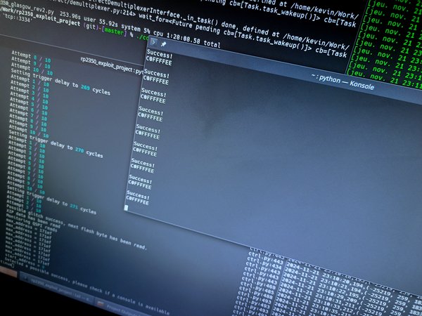
The bypass enables the execution of arbitrary firmware, which can then access secrets stored in the OTP area of the RP2350. This was the objective of Raspberry Pi’s Hacking Challenge.
Possible Improvements
Several elements could be improved to increase the success rate of the attack:
- The laser pulse duration could be fine-tuned. Due to the simple design of the Laser Driver Board, adjusting the pulse duration requires modifying the values of physical components. This process can be cumbersome, so I haven’t thoroughly explored the impact of pulse duration.
- The laser spot size resulting from the Optical Subsystem is relatively large compared to what is typically used in similar attacks. A smaller spot size would likely lead to better-controlled and more repeatable faults.
- The FPGA gateware could be enhanced. Instead of using two physical QSPI flashes, the FPGA could be utilized to emulate one, and dynamically supply the correct data, regardless of the flash address requested after the fault. However, this possibly goes a bit beyond the capabilities of the FPGA I used.
Conclusion
Laser fault injection can be performed on a budget! Although it requires a lot of trial and error, and sourcing a suitable laser source can be tedious, a functional setup can indeed be achieved.
Due to significant compromises, the performance of such a system is not optimal, but interesting results can still be obtained: injecting faults in the RP2350 without triggering its glitch detectors becomes possible.
This alone is not enough to bypass the Secure Boot feature of the RP2350. However, a small but critical section of the Boot ROM has been found to be less hardened and protected by the redundancy co-processor. Injecting a fault at this point, while supplying a compatible payload over the QSPI bus, can essentially defeat the Secure Boot.
While way simpler methods have now been made public, this work still addresses Raspberry Pi’s RP2350 Hacking Challenge.
Additionally, note that it may also be possible to exploit the section of the Boot ROM I targeted without even resorting to LFI. There are some reports of carefully performed EMFI attacks able to bypass the glitch detectors.
The glitch detector is pretty good at detecting EMFI attempts, but it was possible to glitch CPU operations without triggering it with a small coil and a low power glitch
Still, I regret nothing; lasers are fun to play with!
Disclosure
Following my first successful bypass, I immediately contacted Raspberry Pi. For transparency, the documents I shared with them are available here.
Communication with the team was smooth and enjoyable. They acknowledged that the “break-in” was valid and confirmed that the next Boot ROM of the RP2350 would include more hardening around the specific area of the code I targeted.
Bibliography
Andrew 'bunnie' Huang. Infra-red, in-situ (iris) inspection of silicon. 2023. URL: https://arxiv.org/abs/2303.07406, arXiv:2303.07406. ↩
Jemellie Galang, Allesandro Restelli, Edward W. Hagley, and Charles W. Clark. A green laser pointer hazard. 2010. URL: https://arxiv.org/abs/1008.1452, arXiv:1008.1452. ↩
Samuel McDermott, Filip Ayazi, Joel Collins, Joe Knapper, Julian Stirling, Richard Bowman, and Pietro Cicuta. Multi-modal microscopy imaging with the openflexure delta stage. Opt. Express, 30(15):26377–26395, Jul 2022. URL: https://opg.optica.org/oe/abstract.cfm?URI=oe-30-15-26377, doi:10.1364/OE.450211. ↩
Antonios Stylogiannis, Ludwig Prade, Andreas Buehler, Juan Aguirre, George Sergiadis, and Vasilis Ntziachristos. Continuous wave laser diodes enable fast optoacoustic imaging. Photoacoustics, 9:31–38, 2018. URL: https://www.sciencedirect.com/science/article/pii/S2213597917300356, doi:https://doi.org/10.1016/j.pacs.2017.12.002. ↩
