A “Remote” Vulnerability
Posted on Fri 01 June 2018 in Projects
Introduction
A couple of months ago, I spent some time fiddling around my ISP-provided residential gateway. This gateway is actually not just a gateway. It’s more like a mix between a set-top Box and a gateway. Additionally, to access the Internet, the end-user can also use it to watch TV through the HDMI output of the device.
I actually went quite far, and I’ve found a couple of interesting things.
This post won’t go through all of my findings. Instead, I’ll focus on the most “unusual”, educational and interesting one. I’ve indeed found a rather creative way of bypassing (under certain conditions) the WPA2 protection of the gateway’s hotspot. This will involve reverse-engineering, electronics, desoldering things, microcontrollers, and even Software Defined Radio.
Finding and exploiting this flaw allowed me to write a bunch of general purpose tools and even to contribute to the radare2 project. I’m releasing my code along with this article. Hopefully, someone may find it useful.
Please note that the flaws I’ve found have all been reported to my ISP.
They took the issues seriously and quickly fixed them. At the time of writing this blog post, all these vulnerabilities cannot be exploited anymore. Fixed firmwares have been deployed months ago.
Finally, none of the tools released along with this article are able to exploit any of the vulnerabilities.
Hardware Overview
General Features
From an end-user point-of-view, my STB/Gateway has the following and usual features:
- Television and broadband Internet are available through Cable.
- It acts as a residential Gateway. Devices can be connected to with both Ethernet and Wi-Fi. WPA2 is enabled by default.
- It also acts as a Set-Top Box and can be connected to a television monitor. This STB can be controlled thanks to the supplied remote control.
First things first, we’ll start by taking a look at the internals of the STB/Gateway and its remote control. I bought several units on eBay and managed to tear them apart.
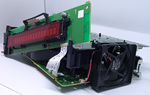
The STB/Gateway is composed of three main printed circuit boards.
Unsurprisingly, one of them is responsible for the “gateway” functionality, while another one is here to act as the STB. The last one contains a screen and a bunch of buttons. It is used as a user interface.
I spent some time studying how these boards were working and communicating together. I’ll now expose what you need to know about them to understand what this entire article is about.
The Gateway Board
We actually won’t do a lot with this board, and I did not spend too much time studying it.
Most of the board’s components are enclosed into board-soldered metallic shields I didn’t bother to remove. The main processor is, for instance, hidden and so is the Wi-Fi module. For the curious readers, I’ve still annotated the following pictures.
A seven ports Ethernet switch. It was under a heat sink.
STB/Gateway connector.
Ethernet connectors.
32M-bit Serial Flash Memory.
2G-bit NAND Flash Memory.
Internet/TV Cable Input.
The main CPU of the Gateway is probably under this heat sink and shield.
Ethernet 1000 Base-T magnetics modules.
RJ11 phone connector. A fixed-line phone can be connected here.
"Single Channel Ringing SLIC (-100 V)" integrated circuit.
SLIC stands for "Subscriber Line Interface Card". This component allows the gateway to interface with a standard fixed-line phone.
Phone line protection diodes.
DC power connector.
Main power on/off button.
USB port.
System reset button.
Pressing this button for a couple a seconds will launch a factory reset.
Metallic shield.
Some WiFi related component is likely to be soldered under, as some tracks escaping from it are connected to UFL connectors on the bottom side of the board.
Metallic shield.
Some WiFi related component is likely to be soldered under, as some tracks escaping from it are connected to UFL connectors on the bottom side of the board.
Metallic shield.
Length matched tracks escaping from it and some termination resistors arrays on the bottom side of the board let me think RAM must hide under.
Ethernet magnetics module.
This component is used for the Ethernet communication between the gateway and the STB boards.
An unconnected 4 pin connector.
Could it be a UART debug port? I actually haven't checked.
An unconnected 4 pin connector.
Could it be a UART debug port? I actually haven't checked.
This board is connected to the STB board through this small piece of circuit board.
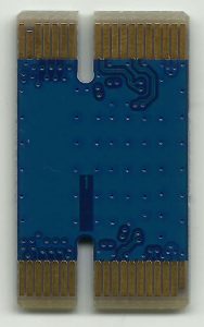
These traces convey both power and various signals. The main communication bus between the STB board and the Gateway Board appears to be Ethernet. Other communication buses seem to include UART, and some GPIOs.
The STB Board
In the scope of this article, the STB part will be far more interesting.
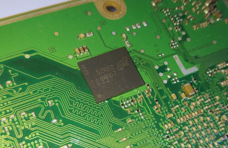
As depicted in the following annotated pictures, the top side of the board is mainly populated with a large processor and some RAM.
An eMMC. It contains the firmware of the STB.
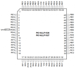
A PIC16F1527 microcontroller.
The CC2534, a 2.4GHz RF radio integrated circuit.
The main STB processor, a Broadcom BCM7252.
The RAM of the STB processor.
4 Samsung DDR3 SDRAM adding up to a total of 2GB of RAM.
STB/Gateway connector.
A "3148LG". No public information available on this component.
It's likely a DVB-C demodulator (DVB-C stands for "Digital Video Broadcasting - Cable").
Internet/TV Cable Input.
Hard Drive SATA connector.
Stereo audio line driver.
A "Security Serial Flash" from Macronix.
I didn't look into it. It seems related to the DVB Conditional Access System.
HDMI Connectors.
USB Connectors.
SD Card Connector.
Analog audio line outputs.
Some power supply circuit.
It's based on a DC-DC regulator from AlphaΩ Semiconductor. It's probably regulating a power-rail useful to the CPU.
A Bluetooth transceiver.
It's based on a Broadcom integrated circuit. Note it's connected to a UFL connector and a ceramic chip antenna.
Some power supply circuit.
It's based on a step-down converter.
Some power supply circuit.
It's based on a step-down converter.
This connector goes to a fan.
This FFC connector goes to the UI board.
This FFC connector goes to a board containing a NFC integrated circuit and antenna.
These pictures depict the most recent revision of the hardware I have.
The main CPU is here a BCM7252 from Broadcom. Little information about it is available online, but according to some press releases, it’s described as a “High performance dual-core Brahma15 10.5K DMIPS CPU”. The Brahma15 seems to be actually close to the Cortex A15 architecture and is compatible with the ARMv7 instruction set.
Interestingly, some former revisions of the board used an x86 processor.
On the bottom side, three interesting components can be found:
- An eMMC
- A PIC microcontroller, the PIC16F1527
- A RF remote communication integrated circuit, the CC2534
Finding an eMMC on such a board is not a surprise. It contains the firmware of the STB. Nevertheless, finding a PIC microcontroller and a RF integrated circuit could sound more surprising.
The PIC Microcontroller
The PIC16F1527 is a small 8-bits microcontroller. It’s here packaged in a 64-PIN TQFP.
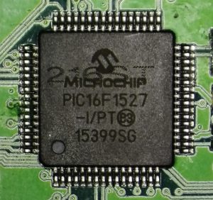
The aim of this PIC, that we’ll from now sometimes refer to as the “MCU” (for Microcontroller Unit), is actually rather simple. It has to handle several simple and low-level functions.
For instance, the MCU is responsible for:
- Handling the buttons of the UI Board (more on this board in the next section)
- Handling the screen of the UI Board
- Communicating with the RF circuit
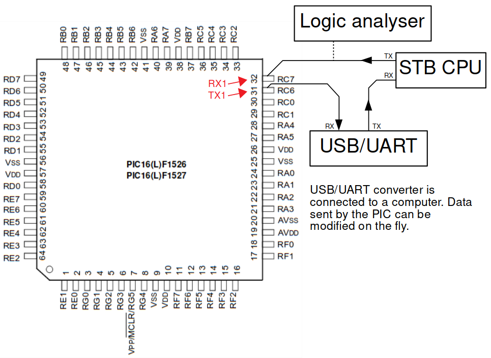
The MCU is communicating with the main STB CPU, that we’ll from now sometimes refer to as the “MPU” (for Microprocessor Unit), and the gateway board via two UART buses.
For instance, when a button on the UI Board is pressed, the MCU will send a couple of bytes to the MPU or to the gateway (depending on which one has been pressed) to inform it this button has been pressed.
Other example: if the MPU needs to update the screen of the UI board, it will do it by sending a command to the MCU.
Thankfully, the datasheet of the PIC16F1527 is freely available online.
The RF Integrated Circuit
The datasheet of the CC2534 is not publicly available. Nevertheless, this part seems pin-to-pin compatible with the CC2533 and seems to have similar features.
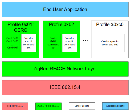
Hence, this IC is, according to its manufacturer Texas Instruments, “A True System-on-Chip Solution for 2.4-GHz IEEE 802.15.4 and ZigBee Applications”. This IC is used to communicate with the remote control.
Indeed, this remote control doesn’t only use a traditional infrared LED to communicate with the STB. The IR communication is only used during the setup of the device. Right after a pairing step, a 2.4-GHz radio protocol called “Zigbee RF4CE” is used.
The Zigbee RF4CE specification offers an immediate, low-cost, easy-to-implement networking solution for control products based on Zigbee Remote Control and Zigbee Input Device. The Zigbee RF4CE specification is designed to provide low-power, low-latency control for a wide range of products including home entertainment devices, garage door openers, keyless entry systems and many more. http://www.zigbee.org/zigbee-for-developers/network-specifications/zigbeerf4ce/
The CC2534 communicates with the MCU via a SPI bus. Hence, key presses transmitted by the remote control are first received by the RF circuit, then by the MCU and finally by the MPU.
The UI Board
This board is populated with the following components:
- A screen, displaying the system’s status.
- Three buttons.
Pressing the buttons will do the following:
- Button 1: Wi-Fi. Used to enable or disable the Wi-Fi.
- Button 2: WPS. Pressing this button allows a device to connect to the Wi-Fi network without the WPA2 key being needed. This feature is enabled by default.
- Button 3: Power. Used to power the STB on and off.
The main unit screen.
The WiFi, WPS, and on/off buttons.
Backlight LEDs for the push buttons.
FFC going from the UI Board to the STB Board.
IR sensor.
Used to receive commands from the remote before the RF4CE pairing has been established.
As I previously said, the screen and push buttons are all connected directly to the MCU who’s in charge of handling these peripherals.
The Remote
The internal of the remote control reveals two main integrated circuits: one of them is a microcontroller I didn’t play around with, while the other one is another CC2534. This CC2534 communicates with the one soldered on the STB board.
As shown in the annotated picture below, one of the board’s side contains these components, while the other side is full of tactile metal dome switches.
A R5F2135CANFP microcontroller (Renesas).
It didn't do a lot with it, but I guess it's safe to assume it's monitoring key presses and is communicating with the CC2534.
The CC2534 integrated circuit.
It's soldered on a PCB module placed on the main remote control PCB.
An infrared LED.
It is used to communicate with the STB before the RF4CE pairing process has been done.
Some pads.
I guess they are used to do some factory testing and to flash the microcontroller.
A speaker, used for a "find my remote" feature.
A FFC connector.
It connects the main PCB to another one, full of additional metallic dome switches.
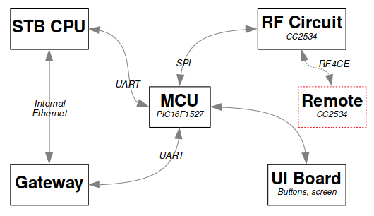
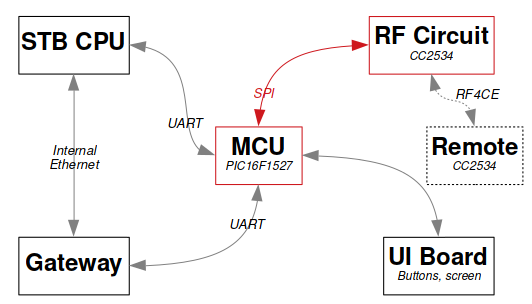
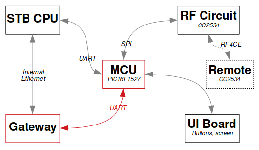
Architecture Summary
The following schematic summarizes the system’s architecture.
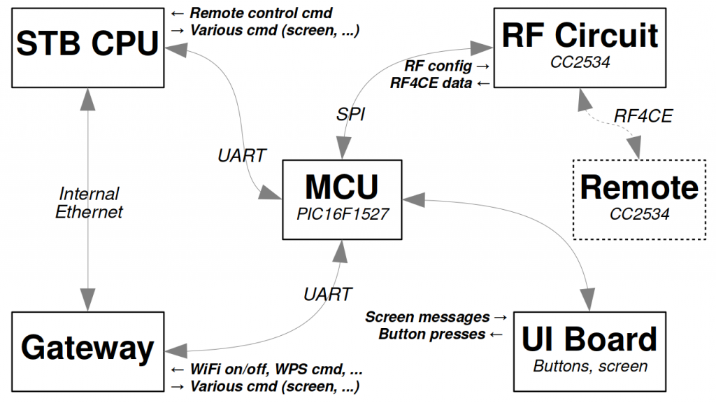
Key points that will be useful for the rest of the article are the following:
- The PIC handles the user interface. It communicates with both the gateway board and the STB board with two distinct UART buses.
- The PIC communicates with the RF integrated circuit, the CC2534, via a SPI bus.
- The CC2534 of the STB board communicates with the CC2534 of the remote control. The radio protocol used is “Zigbee RF4CE”.
Now that the architecture can be understood, let’s discuss the software running on the system. It’s time to dump some firmwares.
Firmware extraction
As I said before, we’ll ignore the firmware running on the gateway board. Instead, we will focus on the code running on the main STB CPU and on the smaller PIC microcontroller.
eMMC Extraction
Let’s start with the firmware of the main CPU. As I said before, this firmware is contained in the eMMC. I didn’t find any clever way to dump this firmware: no talkative UART, …
Instead, as I was able to buy multiple units out of Ebay, I decided to sacrifice one of them. I simply desoldered the eMMC with a hot air reworking station (for anyone interested, I’m using an Atten 858D+. It’s rather cheap, but that was enough).
The footprints of eMMC are standardized by the JEDEC Council. That’s why eMMCs come in a limited number of footprints. The one I desoldered was a 153-balls one. Accordingly, I bought a USB eMMC reader on Aliexpress. I’m well aware cheaper solutions involving fine soldering and a simple SD card reader do exist, but I didn’t want to take the risk of ruining my eMMC.
I was left with a nice memory dump. squasfs partitions can be extracted from it. They contain a Linux root filesystem: binaries, scripts, configuration files, …
The entire Linux system seems to have been designed with security in mind. Binaries are, for instance, hardened with stack smashing detection and read-only relocations. Binary hardening features may not sound like something unusual, but, from my experience, it’s not uncommon for embedded systems to be shipped without these protections. For instance, the device I’ve studied in my previous article came without them. It made binary exploitation way easier.
Additionally, numerous Linux Containers (LXC) are used to fully isolate some processes from others. For instance, once container is dedicated to the STB user interface displayed on the TV, while another one runs a NAS server software, … It means that breaching into one of the STB’s services doesn’t guarantee a full control of the entire system.
At the end of the day, from a pure vulnerability finding point-of-view, studying this Linux system didn’t reveal anything extremely interesting. Nevertheless, I gained a better understanding of the inner workings of the STB. Further, some of the extracted files will actually be useful for what’s coming next.
PIC Firmware Extraction
The PIC Firmware Update Procedure
Now that we’re done with the eMMC, we can start looking at the PIC. My very first idea was to try dumping the PIC’s flash by using the ICSP (In-Circuit Serial Programming) interface. It actually turned out I didn’t need to do that. It could have failed anyway, as the code read-out protection of the PIC was likely activated.
Instead, I realized the STB CPU was actually able to flash the firmware of the PIC. Hence, its firmware must be contained somewhere in the eMMC.
It’s indeed the case. One of the binaries launched at boot is basically doing the following:
- It first checks the version number of the current firmware installed on the PIC. This is done by sending a command via the UART bus.
- If this version doesn’t correspond to the one hardcoded in the binary, it launches the update procedure.
- The new firmware is sent via UART. This firmware image in embedded in the Linux binary.
I simply extracted the PIC firmware image from this binary for further analysis.
PIC Firmware Disassembly
Now that the firmware is available, a way to disassemble it is needed. The PIC16F1527 uses the PIC Enhanced Mid-Range instruction set.
Unfortunately, I didn’t find any disassembler supporting this architecture (IDA Pro only supports midrange instructions and I do not own a license anyway).
That’s why I contributed to the radare2 project and added support for the PIC Enhanced Midrange instruction set. My pull request is available here.
Though, the result and more specifically the automatic analysis of the code isn’t perfect, that’s good enough for our purposes.
Non-destructive PIC Firmware Dumping
As I said before, I bought multiple STB/Gateways out of eBay. Not all of them were using the same PIC software revision. For reasons I’ll explain later, I needed to dump as many PIC firmware revisions as possible. Doing so was of course possible by desoldering all eMMCs and dumping them. Nevertheless, it would have damaged my devices. Another possibility was to wait for an update to be available and sniff the UART communication. Here again, this is not a very practical solution.
Instead, I developed a non-destructive way of dumping this firmware. It required some soldering as well, but it was not as bad as dealing with a huge BGA integrated circuit.
The following is a close up of the PIC UART pins. Conveniently, series resistors are placed along the lines. Desoldering them and soldering them back is easy.
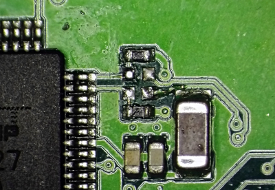
Using a cheap USB to serial converters, it’s possible to intercept and even modify on the fly the serial data going from the PIC to the STB CPU.
As I said before, the CPU STB will trigger an update of the MCU if its firmware version is not matching the expected one. To force an update, we just have to overwrite the PIC’s response to the “get version” UART command.
Using this method, I was able to force updates and dump the firmwares from all the units I bought.
Nevertheless, a part of the PIC’s memory was still missing. Indeed, there is a piece of code in charge of receiving data from the UART port and writing it back to the flash: a custom bootloader. For completeness, I wanted to dump this part as well.
PIC Bootloader Dumping
I first needed to have a clearer idea about how the memory was organized on the flash. Where was the bootloader located? Where was the code I dumped located?
To answer these questions, I tried to disassemble the main firmware image starting from different offsets. The disassembly started to make sense at offset 0x200. Accordingly, I was able to deduce the following simple memory layout.
| Range | Type |
|---|---|
| 0x0000 - 0x01FF | Bootloader |
| 0x0200 - 0x3FFF | Main Code |
To dump this bootloader, I did the following.
I first removed both of the series resistors populated on the UART lines, and connected a USB to UART converter to the PIC. This way, I was able to directly communicate with it.
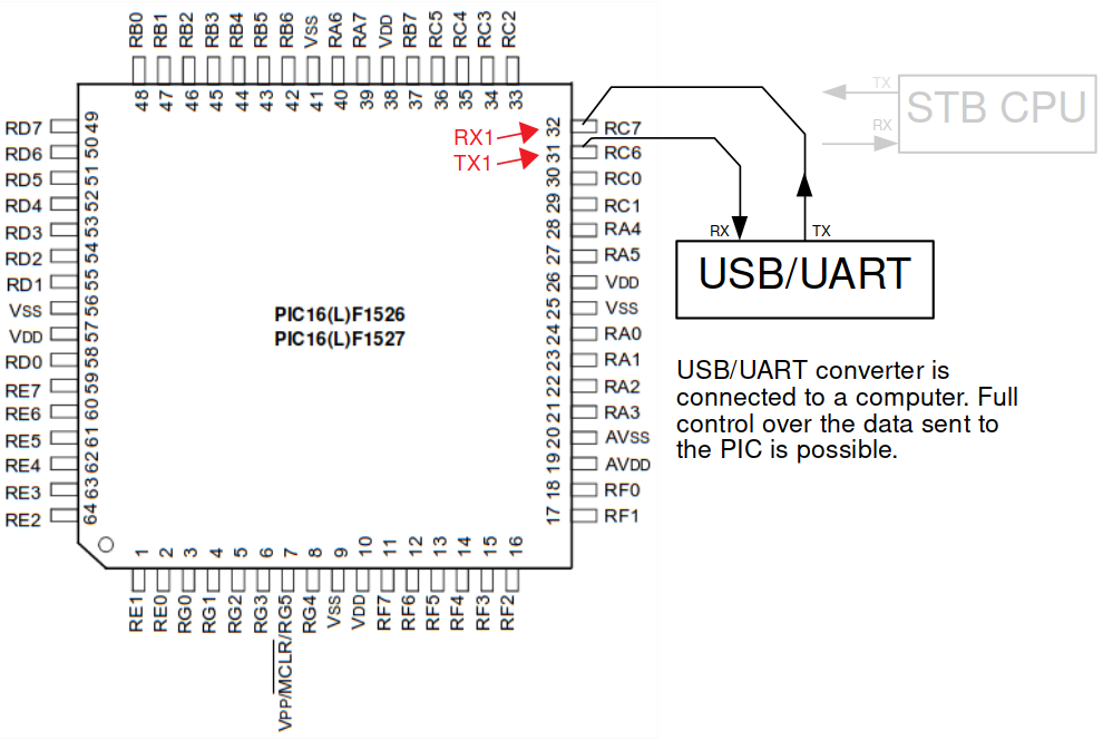
As I was now communicating directly with the PIC, my plan was to upload a custom firmware by using the same communication protocol the MPU was using. This custom firmware could then read the bootloader from the flash and send it via the UART bus.
Nevertheless, I bumped into some difficulties. My first attempts at flashing custom firmwares failed miserably. The PIC refused to run my code and stayed stuck in the bootloader. As I doubted the firmware was signed, I guessed some kind of checksum was used.
The last two bytes of the data sent during the firmware were looking suspicious. Depending on the firmware revision, they were either decoding to an invalid instruction, or to something that didn’t really make sense.
As an example, here is a disassembly of the last few bytes of one of the images I grabbed.
0x00003df0      0800           return
0x00003df2      2100           movlb 0x1
0x00003df4      0430           movlw 0x4
0x00003df6      c901           clr 0x49, f
0x00003df8      2000           movlb 0x0
0x00003dfa      c100           movwf 0x41
0x00003dfc      0800           return
0x00003dfe      5600           invalid    ; "These bytes do not decode to a valid instruction"
0x00003e00      ffff           invalid
0x00003e02      ffff           invalid
0x00003e04      ffff           invalid
0x00003e06      ffff           invalid
And below is another example.
0x00007dae      ed01           clr 0x6d, f
0x00007db0      dc2f           goto 0x7dc
0x00007db2      0230           movlw 0x2
0x00007db4      2100           movlb 0x1
0x00007db6      ed00           movwf 0x6d
0x00007db8      2000           movlb 0x0
0x00007dba      5514           bsf 0x55, 0
0x00007dbc      0800           return
0x00007dbe      8700           movwf 0x7    ; "Weird instruction to end and image. The return just above makes more sense"
0x00007dc0      ffff           invalid
0x00007dc2      ffff           invalid
0x00007dc4      ffff           invalid
It confirmed my intuition about a simple checksum being used. As for how it’s computed, after I tried different things, I realized it was the result of a simple XOR operation between all the bytes of the firmware image and the constant value 0x51.
Knowing the checksum algorithm, it was finally possible to craft a working firmware image. I choose to modify the existing one so that as soon as a key press of the remote control was detected, the bootloader was sent through the UART bus. A part of the injected code is available below. It can be compiled with Microchip’s official assembler mpasmx.
include <p16f1527.inc>

DUMP_CODE CODE 0x38C0

    MOVLB 0x03

    BCF PMCON1, CFGS

    CLRF 0x70
    CLRF 0x71

    ; Loop through the bootloader data
    loop:
        MOVFW 0x70
        MOVWF PMADRL ; Store LSB of address
        MOVFW 0x71
        MOVWF PMADRH ; Store MSB of address

        BSF PMCON1, RD ; Initiate read
        NOP ; Ignored
        NOP ; Ignored

        MOVFW PMDATL
        MOVWF TX1REG

    busy_loop_2:
        BTFSS TX1STA, 1
        GOTO busy_loop_2

        MOVFW PMDATH
        MOVWF TX1REG

    busy_loop_3:
        BTFSS TX1STA, 1
        GOTO busy_loop_3

        INCF 0x70, f
        SKPNZ
        INCF 0x71, f


        MOVFW 0x71
        XORLW 0x20
        SKPNZ
        GOTO resume

        GOTO loop

    ; Use to continue the normal
    ; firmware execution safely
    resume:
        MOVLB 0x2
        BSF 0xC, 3
        BSF 0xF, 0
        RETURN

END
It worked flawlessly, I successfully recovered the entire PIC flash content from all of my devices.
The Remote / STB RF Link
Now that we saw how to grab firmwares, we need to spend some time talking about the communication between the Remote Control and the Set-Top Box. As previously said, the “Zigbee RF4CE” radio protocol is used. I’ll briefly introduce what you need to know about it.
Quick introduction to “Zigbee RF4CE”
RF4CE has been specially designed for remote control applications and is used to transmit small amounts of data at a low speed.
It sits on top of a Physical Layer (PHY) and a Media Access Control (MAC) Layer, both defined by the IEEE 802.15.4.
The PHY Layer
Data is transmitted on the 2.4GHz ISM Band.
RF4CE is only using 3 channels out of the 16 2.4GHz possible Zigbee channels. Used channels are channels 15, 20 and 25, respectively corresponding to frequencies 2425MHz, 2450MHz and 2475MHz.
The modulation used is O-QPSK. Noisy immunity is improved thanks to DSSS.
The MAC Layer
The general structure of a Zigbee packet is the following.
| Size (bytes) | 2 | 1 | 0 or 2 | 0, 2 or 8 | 0 or 2 | 0, 2 or 8 | * | 2 |
|---|---|---|---|---|---|---|---|---|
| Field | Frame Control | Sequence Number | Destination PAN | Destination Address | Source PAN | Source Address | Payload | Checksum |
Specifically, the Frame Control is composed of the following fields:
| Bit index | 0-2 | 3 | 4 | 5 | 6 | 7-9 | 10-11 | 12-13 | 14-15 |
|---|---|---|---|---|---|---|---|---|---|
| Field | Frame Type | Security Enable | Frame Pending | ACK | Intra PAN | Reserved | Destination Addressing Mode | Reserved | Source Addressing Mode |
All these fields won’t be useful for our purpose. Here is what we should keep in mind to understand some of the things I’ll further describe:
- Frame control, bit 10-11 and 14-15: Different addressing modes can be used for the source and the destination. A
longaddressing mode means source or destination addresses will be composed of 8 bytes, while ashortaddressing means only two bytes will be used. PANstands for Personal Area Network. This concept is specific to Zigbee. Basically, a Zigbee node is only allowed to send data to a node from the samePAN.- In our case, the
Frame Payloadwill contain the RF4CE Layer.
The RF4CE Layer
A RF4CE Frame has the following format.
| Size (bytes) | 1 | 4 | 0 or 1 | 0 or 2 | * | 0 or 4 |
|---|---|---|---|---|---|---|
| Field | Frame Control | Frame Counter | Profile Identifier | Vendor Identifier | Frame Payload | Message Integrity Code |
More specifically, the Frame Control byte has this structure.
| Bit index | 0-1 | 2 | 3-4 | 5 | 6-7 |
|---|---|---|---|---|---|
| Field | Frame Type | Security Enable | Protocol Version | Reserved | Channel Designator |
Here again, not everything will be useful for this article. Let’s focus on the important fields.
- The
Frame Typecan take several values. Some frames are Command frames used for instance during the pairing process. Others are Data frames. Most of the time, the remote is sending Data frames to the STB. - There is a
Security Enablebit. When set to ‘1’, theFrame Payloadwill be ciphered with what’s called AES-128-CCM*. This algorithm is described by the RF4CE specification. AMessage Integrity Codewill be appended at the end of the frame. Our remote does always use RF4CE security after the pairing process.
The AES-128-CCM* is a derivative of the CCM mode of operation and uses AES as the block cipher. The key is 128 bits long.
This key is exchanged between two devices during the pairing process. The process is a bit “obfuscated” but everything is basically cleartext.
The idea is to split the key into 37 seeds and to compute the key by using the following XOR operations.
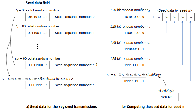
To make everything more difficult for an attacker to sniff, the Zigbee packets transporting the key seeds are sent with a very low output power.
Needless to say that this key exchange procedure is not perfect. It has already been widely criticized. Nevertheless, if the pairing process is not sniffed by an attacker, no major issues have been discovered with AES-128-CCM* so far.
In the case of our remote and STB, this pairing process and key exchange only happens once, during the first boot of the STB.
RF4CE Tools
I wrote a couple of tools to play with RF4CE packets. They are all available on this GitHub repository.
For maximum flexibility, these tools are all built around SDR (Software Defined Radio) technology.
They do have the following features:
- RF4CE packets parsing and crafting. This includes support for the AES-128-CCM* cryptographic algorithm used by RF4CE devices after the pairing process.
- RF4CE packets sniffing. This includes deciphering packets in case the ciphering key is known. This key can be computed in case the pairing process can be sniffed.
- RF4CE packets injection.
My code is based on:
- GNU Radio
- The IEEE 802.15.4 MAC and PHY layers are provided by the gr-ieee802-15-4 project
I’ve successfully tested these tools with both a HackRF and a newer PlutoSDR.
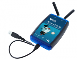
Please note that a device like the PlutoSDR supports full-duplex communication. That’s why after it has sent a packet, it can immediately wait for a ACK from the receiver and try to switch frequency if this packet is not acknowledged.
The HackRF on the other side is only half-duplex and cannot do that. I haven’t found a way to switch between RX and TX modes fast enough to handle ACK packets.
In other words, only the PlutoSDR can handle the frequency agility feature of the RF4CE protocol.
I’ll now give some more details about how to use these tools.
If you aren’t interested in them, you can skip this section. It won’t keep you from understanding the rest of the article.
Sniffer
The Python script to launch the sniffer is called sniffer.py.
$ ./sniffer.py -h
usage: sniffer.py [-h] [-l LINK] [-c {15,20,25}] [-s {hackrf,pluto-sdr}]

optional arguments:
  -h, --help            show this help message and exit
  -l LINK, --link LINK  JSON file containing link information
  -c {15,20,25}, --channel {15,20,25}
                        RF4CE channel (default: 15)
  -s {hackrf,pluto-sdr}, --sdr {hackrf,pluto-sdr}
                        SDR Device to use (default: pluto-sdr)
The channel and sdr arguments are straightforward. The link argument let you specify a path to a configuration file.
This file is a JSON formatted file containing information about a RF4CE communication: the addresses of the nodes, the ciphering key in use, …
The file may for instance look like the following:
{
    "full_destination": "00:12:4b:00:0a:77:f0:a5",
    "short_source": "0x7df9",
    "key": "69f34a813d4b444b2c89feaef796f3e9",
    "full_source": "00:12:4b:00:09:0e:dd:0c",
    "dest_panid": "0x9304",
    "short_destination": "0xdc3",
    "frame_counter": 457781
}
Here is a quick shot at what the output looks like while sniffing the RF4CE link between the remote and the STB and pressing some keys.
$ ./sniffer.py -l secured.json -c 25
Link configuration:
    Loaded from 'secured.json'
    Source: 00:12:4b:00:09:0e:dd:0c - 0x7df9
    Destination: 00:12:4b:00:0a:77:f0:a5 - 0xdc3
    Panid: 0x9304
    Key: 69f34a813d4b444b2c89feaef796f3e9
    Frame Counter: 457781
[!] Sniffing on channel 25
[!] Sniffing...

------ 2018-04-02 20:06:23.569120 ------
Full packet data: 6188220493c30df97d2d37cf0100019e14308ec727e9fb
###[ 802.15.4 ]###
  fcf_panidcompress= True
  fcf_ackreq= True
  fcf_pending= False
  fcf_security= False
  fcf_frametype= Data
  fcf_srcaddrmode= Short
  fcf_framever= 0
  fcf_destaddrmode= Short
  seqnum= 34
###[ 802.15.4 Data ]###
     dest_panid= 0x9304
     dest_addr= 0xdc3
     src_addr= 0x7df9
###[ Raw ]###
        load= "-7\xcf\x01\x00\x01\x9e\x140\x8e\xc7'"
###[ RF4CE ]###
(00:12:4b:00:09:0e:dd:0c - 0x7df9) -> (00:12:4b:00:0a:77:f0:a5 - 0xdc3) : [DATA - profile:0x1 - counter:0x1cf37] : 0102

------ 2018-04-02 20:06:23.572180 ------
Full packet data: 020022a8b7
###[ 802.15.4 ]###
  fcf_panidcompress= False
  fcf_ackreq= False
  fcf_pending= False
  fcf_security= False
  fcf_frametype= Ack
  fcf_srcaddrmode= None
  fcf_framever= 0
  fcf_destaddrmode= None
  seqnum= 34

------ 2018-04-02 20:06:23.687356 ------
Full packet data: 6188230493c30df97d2d38cf0100015174ad12dd74c0ae
###[ 802.15.4 ]###
  fcf_panidcompress= True
  fcf_ackreq= True
  fcf_pending= False
  fcf_security= False
  fcf_frametype= Data
  fcf_srcaddrmode= Short
  fcf_framever= 0
  fcf_destaddrmode= Short
  seqnum= 35
###[ 802.15.4 Data ]###
     dest_panid= 0x9304
     dest_addr= 0xdc3
     src_addr= 0x7df9
###[ Raw ]###
        load= '-8\xcf\x01\x00\x01Qt\xad\x12\xddt'
###[ RF4CE ]###
(00:12:4b:00:09:0e:dd:0c - 0x7df9) -> (00:12:4b:00:0a:77:f0:a5 - 0xdc3) : [DATA - profile:0x1 - counter:0x1cf38] : 0202

------ 2018-04-02 20:06:23.691351 ------
Full packet data: 02002321a6
###[ 802.15.4 ]###
  fcf_panidcompress= False
  fcf_ackreq= False
  fcf_pending= False
  fcf_security= False
  fcf_frametype= Ack
  fcf_srcaddrmode= None
  fcf_framever= 0
  fcf_destaddrmode= None
  seqnum= 35

------ 2018-04-02 20:06:23.755723 ------
Full packet data: 6188240493c30df97d2d39cf01000131ba320f02e273bd
###[ 802.15.4 ]###
  fcf_panidcompress= True
  fcf_ackreq= True
  fcf_pending= False
  fcf_security= False
  fcf_frametype= Data
  fcf_srcaddrmode= Short
  fcf_framever= 0
  fcf_destaddrmode= Short
  seqnum= 36
###[ 802.15.4 Data ]###
     dest_panid= 0x9304
     dest_addr= 0xdc3
     src_addr= 0x7df9
###[ Raw ]###
        load= '-9\xcf\x01\x00\x011\xba2\x0f\x02\xe2'
###[ RF4CE ]###
(00:12:4b:00:09:0e:dd:0c - 0x7df9) -> (00:12:4b:00:0a:77:f0:a5 - 0xdc3) : [DATA - profile:0x1 - counter:0x1cf39] : 0302

------ 2018-04-02 20:06:23.757264 ------
Full packet data: 0200249ed2
###[ 802.15.4 ]###
  fcf_panidcompress= False
  fcf_ackreq= False
  fcf_pending= False
  fcf_security= False
  fcf_frametype= Ack
  fcf_srcaddrmode= None
  fcf_framever= 0
  fcf_destaddrmode= None
  seqnum= 36

------ 2018-04-02 20:06:25.372381 ------
Full packet data: 6188250493c30df97d2d3acf010001d0dbc2daafadab98
###[ 802.15.4 ]###
  fcf_panidcompress= True
  fcf_ackreq= True
  fcf_pending= False
  fcf_security= False
  fcf_frametype= Data
  fcf_srcaddrmode= Short
  fcf_framever= 0
  fcf_destaddrmode= Short
  seqnum= 37
###[ 802.15.4 Data ]###
     dest_panid= 0x9304
     dest_addr= 0xdc3
     src_addr= 0x7df9
###[ Raw ]###
        load= '-:\xcf\x01\x00\x01\xd0\xdb\xc2\xda\xaf\xad'
###[ RF4CE ]###
(00:12:4b:00:09:0e:dd:0c - 0x7df9) -> (00:12:4b:00:0a:77:f0:a5 - 0xdc3) : [DATA - profile:0x1 - counter:0x1cf3a] : 0101

------ 2018-04-02 20:06:25.375149 ------
Full packet data: 02002517c3
###[ 802.15.4 ]###
  fcf_panidcompress= False
  fcf_ackreq= False
  fcf_pending= False
  fcf_security= False
  fcf_frametype= Ack
  fcf_srcaddrmode= None
  fcf_framever= 0
  fcf_destaddrmode= None
  seqnum= 37

------ 2018-04-02 20:06:25.490058 ------
Full packet data: 6188260493c30df97d2d3bcf01000127e203ce16d8fd21
###[ 802.15.4 ]###
  fcf_panidcompress= True
  fcf_ackreq= True
  fcf_pending= False
  fcf_security= False
  fcf_frametype= Data
  fcf_srcaddrmode= Short
  fcf_framever= 0
  fcf_destaddrmode= Short
  seqnum= 38
###[ 802.15.4 Data ]###
     dest_panid= 0x9304
     dest_addr= 0xdc3
     src_addr= 0x7df9
###[ Raw ]###
        load= "-;\xcf\x01\x00\x01'\xe2\x03\xce\x16\xd8"
###[ RF4CE ]###
(00:12:4b:00:09:0e:dd:0c - 0x7df9) -> (00:12:4b:00:0a:77:f0:a5 - 0xdc3) : [DATA - profile:0x1 - counter:0x1cf3b] : 0201

------ 2018-04-02 20:06:25.493336 ------
Full packet data: 0200268cf1
###[ 802.15.4 ]###
  fcf_panidcompress= False
  fcf_ackreq= False
  fcf_pending= False
  fcf_security= False
  fcf_frametype= Ack
  fcf_srcaddrmode= None
  fcf_framever= 0
  fcf_destaddrmode= None
  seqnum= 38

------ 2018-04-02 20:06:25.557888 ------
Full packet data: 6188270493c30df97d2d3ccf010001528fd2b6d943f2df
###[ 802.15.4 ]###
  fcf_panidcompress= True
  fcf_ackreq= True
  fcf_pending= False
  fcf_security= False
  fcf_frametype= Data
  fcf_srcaddrmode= Short
  fcf_framever= 0
  fcf_destaddrmode= Short
  seqnum= 39
###[ 802.15.4 Data ]###
     dest_panid= 0x9304
     dest_addr= 0xdc3
     src_addr= 0x7df9
###[ Raw ]###
        load= '-<\xcf\x01\x00\x01R\x8f\xd2\xb6\xd9C'
###[ RF4CE ]###
(00:12:4b:00:09:0e:dd:0c - 0x7df9) -> (00:12:4b:00:0a:77:f0:a5 - 0xdc3) : [DATA - profile:0x1 - counter:0x1cf3c] : 0301

------ 2018-04-02 20:06:25.559497 ------
Full packet data: 02002705e0
###[ 802.15.4 ]###
  fcf_panidcompress= False
  fcf_ackreq= False
  fcf_pending= False
  fcf_security= False
  fcf_frametype= Ack
  fcf_srcaddrmode= None
  fcf_framever= 0
  fcf_destaddrmode= None
  seqnum= 39
^C[!] Exiting...
Pairing Sniffer
The Python script to launch the “pairing sniffer” is called pairing_sniffer.py.
This “pairing sniffer” can be used to generate the JSON file I talked about in the previous section.
$ ./pairing_sniffer.py -h
usage: pairing_sniffer.py [-h] [-c {15,20,25}] [-s {hackrf,pluto-sdr}]
                          output_file

positional arguments:
  output_file           output JSON file storing link information

optional arguments:
  -h, --help            show this help message and exit
  -c {15,20,25}, --channel {15,20,25}
                        RF4CE channel (default: 15)
  -s {hackrf,pluto-sdr}, --sdr {hackrf,pluto-sdr}
                        SDR Device to use (default: pluto-sdr)
It sniffs and analyzes the pairing packets and extracts useful information from them. If all the “key exchange” commands are successfully sniffed, it can compute the link’s AES-128-CCM* encryption key.
Packet Injection
The Python script to launch to inject arbitrary RF4CE packets is called injector.py.
$ ./injector.py -h
usage: injector.py [-h] [-c {15,20,25}] [-s {hackrf,pluto-sdr}] config_file

positional arguments:
  config_file           JSON file containing link information

optional arguments:
  -h, --help            show this help message and exit
  -c {15,20,25}, --channel {15,20,25}
                        RF4CE channel (default: 15)
  -s {hackrf,pluto-sdr}, --sdr {hackrf,pluto-sdr}
                        SDR Device to use (default: pluto-sdr)
The RF4CE link will be configured according to the supplied JSON configuration file. If a key is supplied in this file, payloads will be fully decrypted.
Launching the script will provide access to an interactive prompt from where commands and RF4CE payloads can be entered.
Below is a short example session.
$ ./injector.py secured.json -c 15 -s hackrf
Link configuration:
    Loaded from 'secured.json'
    Source: 00:12:4b:00:09:0e:dd:0c - 0x7df9
    Destination: 00:12:4b:00:0a:77:f0:a5 - 0xdc3
    Panid: 0x9304
    Key: 69f34a813d4b444b2c89feaef796f3e9
    Frame Counter: 457781
[!] [2018-04-02 21:04:53.184542] SRC:(00:12:4b:00:09:0e:dd:0c - 0x7df9) -> DST:(00:12:4b:00:0a:77:f0:a5 - 0xdc3)
[!] [2018-04-02 21:04:53.184586] Loading last frame counter: 457781

    Available commands:

        counter <value>      Set the frame counter value

        delay <value>        Minimum delay between packet (seconds)

        ciphered [0, 1]      Send AES ciphered payloads of cleartext payloads.
                             Only possible if a key has been configured

        profile <profile>    Select a profile number

        exit

    Other inputs will be considered as data to be sent.

(457781 - 0x01 - ciphered)>>> 01020304
[!] [2018-04-02 21:04:58.886987] Transmitting 6188010493c30df97d2d36fc060001ba92a47bfa13813eab10
(457782 - 0x01 - ciphered)>>> ciphered 0
[!] [2018-04-02 21:05:02.321507] Set ciphered to False
(457782 - 0x01 - plain)>>> 01020304050607
[!] [2018-04-02 21:05:08.485063] Transmitting 6188020493c30df97d2937fc06000101020304050607a34f
(457783 - 0x01 - plain)>>> exit
[!] [2018-04-02 21:05:10.825454] Saving last frame counter: 457783
Detailed Remote / STB Communication
Now that we understand more about RF4CE, let’s provide details about what happens from the moment one of the keys of the remote control is pressed to the moment this information arrives to the STB MPU.
Step 1: A key is pressed on the remote
A key is pressed on the remote control. This key pressed will be detected by the microcontroller of the remote.
This same microcontroller will command the CC2534 over the SPI bus to send a data packet corresponding to this key.
For the sake of the example, we will suppose the “Enter” key has been pressed. It corresponds to the payload 0201.
Step 2: The RF4CE packet
The RF4CE is generated by the CC2534. RF4CE security is enabled. It means the RF4CE payload is ciphered, and a Message Integrity Code is used at the end of the RF4CE frame. The ciphering key used has been exchanged a long time ago during the pairing process.
This frame is encapsulated into a 802.15.4 packet.
When transmitted over the air, the Zigbee packet and encapsulated RF4CE frame look like the following:
| Full packet | Frame Control | Seq Number | Dest PAN | Dest Address | Src Address | Payload | Checksum |
|---|---|---|---|---|---|---|---|
| 0x8861 | 0x26 | 0x9304 | 0x0dc3 | 0x7df9 | 2d3bcf01000127e203ce16d8 | 0x21fd | |
| Frame Type | 0b001 (data) | ||||||
| Security Enable | 0b0 | ||||||
| Frame Pending | 0b0 | ||||||
| ACK | 0b1 | ||||||
| Intra PAN | 0b1 | ||||||
| Reserved | 0b000 | ||||||
| Dest Addressing Mode | 0b10 (short) | ||||||
| Reserved | 0b00 | ||||||
| Src Addressing Mode | 0b10 (short) |
| RF4CE Frame | Frame Control | Frame Counter | Profile Identifier | Frame Payload | Message Integrity Code |
|---|---|---|---|---|---|
| 0x2d | 0x0001cf3b | 0x01 | 27e2 | 03ce16d8 | |
| Frame Type | 0b01 (data) | ||||
| Security Enable | 0b1 | ||||
| Protocol Version | 0b01 | ||||
| Reserved | 0b1 | ||||
| Channel Designator | 0b00 |
Step 3: Receiving the packet
This packet is received by the CC2534 of the STB. It’s parsed and deciphered by this same component before being sent via the SPI bus to the PIC microcontroller.
Let’s spend more time studying the SPI communication between these two components.
The CC2534 actually embeds an 8051 Microcontroller core, which I’ve found to be running RemoTI. RemoTI is Texas Instruments’ own “RF4CE Compliant Protocol Stack”. The SPI interface protocol documentation is freely available.
In our case, a ReceiveData command will be issued by the CC2534. According to the RemoTI documentation, the structure of this command is the following.
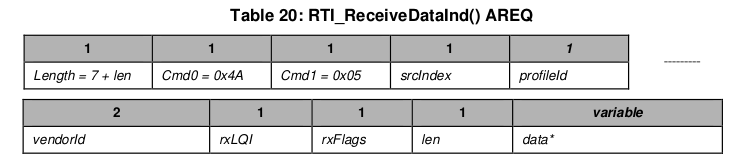
For the payload corresponding to our key press, the values actually transmitted over the SPI bus are:
| Length | Cmd0 | Cmd1 | srcIndex | profileID | vendorId | rxLQI | rxFlags | len | data |
|---|---|---|---|---|---|---|---|---|---|
| 0x09 | 0x4a | 0x05 | 0x00 | 0x01 | 0x0000 | 0x94 | 0x01 | 0x02 | 0201 |
Step 4: From the MCU to the MPU
The transmitted SPI data is parsed by the PIC microcontroller. It will then send the corresponding command to the STB MPU via the UART bus. For us, the detailed format of these UART commands won’t matter.
Vulnerability in the RF4CE Implementation
As previously stated, the remote control uses a secure link to talk to the STB. RF4CE payload are encrypted and authenticated thanks to the AES-128-CCM* algorithm. Hence, an attacker sniffing the packet won’t be able to understand the RF4CE payload. It’s interesting to notice that only the payloads are ciphered. Everything else is plain-text.
According to the RF4CE specification, once a secure link is established between two nodes, unsecured packets should be dropped. In our system, this is not the case.
No matter whether the received frame is ciphered or not, the CC2534 will process it and transmit it via the SPI bus. Nevertheless, it should still possible for the MCU to know whether a frame is secured or not. Indeed, when secured data is received, the rxFlags field of the SPI frame sent by the CC2534 is supposed to reflect it.
However, the firmware of the MCU isn’t actually checking this rxFlags. Unsecured and secured payloads are both accepted and processed in the same way.
To sump up, unsecured packets are accepted and processed by the STB, even though a secure link has been established. It means RF4CE packet injection is possible.
The attacker will first need to sniff some legitimate traffic between the remote and the STB. The STB address, remote address, PAN identifier or frame counter can all be extracted from this traffic, even if AES-128-CCM* is used.
Next, clear-text packets can be crafted by the attacker. The Security Enable field of the RF4CE Frame Control just has to be set to ‘0’.
To conclude, it means that even though the attacker cannot know which keys are pressed by the victim, he is still able to communicate with the STB.
At first, it may look like a rather minor issue: what can the attacker do anyway? Switch channels? Increase the volume? It doesn’t look that scary. Nevertheless, by reading the next section of this blog post, you will understand that with this specific STB/Gateway, it can go way beyond this.
The PIC Buffer Overflow
Introduction
As, injecting RF4CE packets was possible, I started fuzzing the STB by sending it crafted packets.
I quickly noticed that sending large RF4CE data frames was sometimes having surprising effects on the PIC. Depending on the length and content of the payload data, the microcontroller was sometimes freezing or even resetting.
It obviously looked like a buffer overflow. But how to exploit a buffer overflow on a PIC microcontroller? Is there anything “evil” to achieve, considering this PIC is only used for basic functions?
To answer these questions, I’ll first have to introduce the basics of the PIC Enhanced Midrange architecture. Readers already familiar with it may feel free to skip this section. I’ll then highlight points that make “exploiting” a buffer overflow on such a device tricky.
The PIC Midrange Architecture
Instruction Set
The PIC Enhanced Midrange Architecture supports 49 instructions encoded on 14-bits.
I won’t spend much time detailing these instructions.
Instead, on all the following assembly listing of this article, you can just hover every instruction to make of screenshot of the relevant documentation appear.
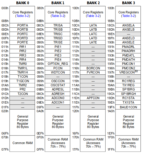
Memory Layout
The PIC Enhanced Midrange Architecture is a Harvard Architecture. It means that instruction memory is separated from data memory.
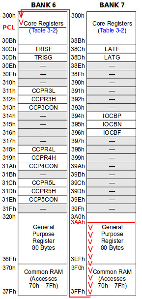
The PIC data memory is divided into several 128 bytes banks. All banks have the same structure detailed in the following table.
| Address Range | Memory Type |
|---|---|
| 0x000 - 0x00b | Core Registers |
| 0x00c - 0x01f | Peripherals Registers |
| 0x020 - 0x06f | General Purpose Registers |
| 0x070 - 0x07f | Common RAM |
For instance, this figure extracted from the datasheet of our PIC shows the first 4 available Data Memory banks.
Let’s detail these memory areas.
The Core Registers
The Core Registers are accessible from all banks. These registers are the following.
| Address | Register |
|---|---|
| 0x00 | INDF0 |
| 0x01 | INDF1 |
| 0x02 | PCL |
| 0x03 | STATUS |
| 0x04 | FSR0L |
| 0x05 | FSR0H |
| 0x06 | FSR1L |
| 0x07 | FSR1H |
| 0x08 | BSR |
| 0x09 | WREG |
| 0x0a | PCLATH |
| 0x0b | INTCON |
The INDFn, FSRnL and FSRnH registers are used for something called Indirect Memory Addressing. It will be explained in the following sections.
The PCL and PCLATH are used to store the program counter. The behavior of these registers will be very important for us and will be detailed in the next section.
The WREG register is the Working Register. This register is used as one of the operands of most arithmetic and logic instructions. There’s only one working register.
The BSR register is the Bank Select Register. The value stored inside this register is the currently selected memory bank index. Let’s take a look at the following pieces of code to understand what it means.
0x00000000 2002movlb0x0 0x00000001 1008movf0x10, w
The first instruction sets the value of BSR to 0x00, which means the bank 0 is selected. The second instruction loads a byte from the memory to WREG. Here, as Bank 0 is selected, the value corresponding to the register PORTE is loaded.
0x00000000 2002movlb0x2 0x00000001 1008movf0x10, w
Here, the selected bank is the bank 2. It means the value of LATE will be used.
The Peripherals Registers
The Peripherals Registers are used to interact with the hardware peripherals of the PIC. For instance, UART, SPI or GPIOs are all controlled by reading and writing values to these registers.
The General Purpose Registers
Nothing fancy here, the General Purpose Registers are simply used to store and read data.
The Common RAM Registers
Same as above, the Common RAM Registers are used to store a read data. Nevertheless, this memory area is common to all banks. No matter which bank is selected, the accessed bytes will be the same.
The PCL and PCLATH registers
The PCL is storing the LSB of the program counter, while the PCLATH is storing the MSB. It’s possible to directly write to these registers. Let’s, for instance, take a look at the following.
0x00000000 8831movlp0x8 0x00000001 4230movlw0x42 0x00000002 8200movwfPCL
The first instruction will load the PCLATH register to 0x08. This won’t alter the execution flow of the program, the following instruction is still executed. WREG is next set to 0x42. Finally, PCL is set to the value of WREG.
When PCL is altered this way, the execution flow is modified according to the values of both PCL and PCLATH. In this case, the PIC will jump to the instruction located ad 0x0842.
Indirect Memory Addressing
So far, we’ve always accessed the Data Memory by directly addressing it. It’s also possible to use the special core registers INDFn, FSRnL and FSRnH to do what’s called Indirect Memory Addressing. The following listing gives an example of this addressing mode.
0x00000000 0130movlw0x1 0x00000001 8400movwfFSR0L 0x00000002 2030movlw0x20 0x00000003 8500movwfFSR0H 0x00000004 0008movfINDF0, w
FSR0L is set to 0x01 and FSR0H to 0x20. Consequently, accessing INDF0 will access data memory at address 0x120. This piece of code is equivalent to:
0x00000000 2200movlb0x2 0x00000002 2008movf0x20, w
Challenges of a PIC Buffer Overflow Exploit
Introduction
Exploiting a buffer overflow on this PIC differs from the “usual” ARM or x86 binary exploitation we’re used to.
As I said before, we’re facing a Harvard Architecture. Code and data being in two different address spaces, things related to shellcodes are not an option.
Further, the PIC16F1527 call stack is not located on the Data Memory. This call stack is a hardware call stack that cannot be addressed like the Data Memory. Exploiting this target won’t exactly be about overwriting a return address.
The SPI_transmit function
To better understand what’s going on, we’ll need to take a look at the disassembly of the low-level function in charge of receiving the RF4CE payload from SPI data of the CC2534. If we examine the SPI frame we described in the previous section, the data read by the call we’re interested in is the highlighted data.
| Length | Cmd0 | Cmd1 | srcIndex | profileID | vendorId | rxLQI | rxFlags | len | data |
|---|---|---|---|---|---|---|---|---|---|
| 0x09 | 0x4a | 0x05 | 0x00 | 0x01 | 0x0000 | 0x94 | 0x01 | 0x02 | 0201 |
This assembly listing is available below.
┌───────────────────────┐
│ (fcn) SPI_transmit 52 │
│ SPI_transmit (); │
│ movwf 0x33 │
└───────────────────────┘
│
┌───────────┘
┌──────────┐
│ │
│ │
│ ┌──────────────────────────────────────────────┐
│ │ decf
0x33 │
└───────────────────────┘
│
┌───────────┘
┌──────────┐
│ │
│ │
│ ┌──────────────────────────────────────────────┐
│ │ decf 0x32, f │
│ │ movf
0x32, f │
│ │ movf 0x32, w │
│ │ xorlw
0x32, w │
│ │ xorlw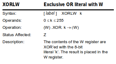 0xff │
│ │ btfsc
0xff │
│ │ btfsc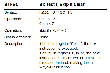 0x3, 2 │
│ └──────────────────────────────────────────────┘
│ │ │
│ │ └─────────────────────┐
│ │ │
│ │ │
│ ┌────────────────────┐ ┌────────────────────┐
│ │ return
0x3, 2 │
│ └──────────────────────────────────────────────┘
│ │ │
│ │ └─────────────────────┐
│ │ │
│ │ │
│ ┌────────────────────┐ ┌────────────────────┐
│ │ return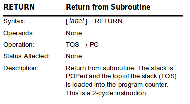 │ │ movf 0x33, w │
│ └────────────────────┘ │ movwf FSR1L │
│ │ movlw
│ │ movf 0x33, w │
│ └────────────────────┘ │ movwf FSR1L │
│ │ movlw 0x3 │
│ │ movwf FSR1H │
│ │ movf INDF1, w │
│ │ movlb
0x3 │
│ │ movwf FSR1H │
│ │ movf INDF1, w │
│ │ movlb 0x4 │
│ │ movwf SSP2BUF │
│ └────────────────────┘
│ │
│ ┌──────────────────────────────┘
│┌────┐
││ │
││ │
││┌──────────────────────────────────────────────┐
│││ btfss
0x4 │
│ │ movwf SSP2BUF │
│ └────────────────────┘
│ │
│ ┌──────────────────────────────┘
│┌────┐
││ │
││ │
││┌──────────────────────────────────────────────┐
│││ btfss SSP2STAT, 0 │
││└──────────────────────────────────────────────┘
││ │ │
││ │ └──────────────────────────┐
││ └────┐ │
││ │ │
││ │ │
││ ┌────────────────────┐ ┌────────────────────┐
││ │ goto
SSP2STAT, 0 │
││└──────────────────────────────────────────────┘
││ │ │
││ │ └──────────────────────────┐
││ └────┐ │
││ │ │
││ │ │
││ ┌────────────────────┐ ┌────────────────────┐
││ │ goto 0x4cd │ │ movlb 0x0 │
││ └────────────────────┘ │ movf 0x33, w │
││ │ │ movwf FSR1L │
││ │ │ movlw 0x3 │
││ │ │ movwf FSR1H │
││ │ │ movlb 0x4 │
││ │ │ movf SSP2BUF, w │
││ │ │ movwf INDF1 │
││ │ │ movlb 0x0 │
││ │ │ incf
0x4cd │ │ movlb 0x0 │
││ └────────────────────┘ │ movf 0x33, w │
││ │ │ movwf FSR1L │
││ │ │ movlw 0x3 │
││ │ │ movwf FSR1H │
││ │ │ movlb 0x4 │
││ │ │ movf SSP2BUF, w │
││ │ │ movwf INDF1 │
││ │ │ movlb 0x0 │
││ │ │ incf 0x33, f │
││ │ │ goto 0x4c1 │
││ │ └────────────────────┘
││ │ │
│└─────────┘ │
└────────────────────────────────────┘
0x33, f │
││ │ │ goto 0x4c1 │
││ │ └────────────────────┘
││ │ │
│└─────────┘ │
└────────────────────────────────────┘
The following table gave the values of relevant memory bytes when this function is called.
| Address / Register | Value |
|---|---|
| 0x032 | RF4CE Frame Payload Size |
| WREG | 0xAA |
| PCLATH | 0x03 |
| BSR | 0x00 |
Let’s study this function step by step.
- First, the value
WREGis stored at address0x033(bank 0, offset0x33). This value is actually the LSB byte of a pointer to the data buffer aimed at storing the RF4CE payload. - Next, the main loop is entered. The
RF4CE Frame Payload Sizevariable stored at0x033is decreased, and a check is made to know whether more data can be received or not. The value of theRF4CE Frame Payload Sizeis a parameter of this function. It has been retrieved by receiving the first bytes of the SPI data sent by the CC2534. As you may expect, no boundary checking is done against this value. - Data bytes are fetched from addresses starting a
0x3AAby using the Indirect Addressing method. This byte is next loaded into theSSP2BUSperipheral register. - As soon as this register is written, the SPI transfer begins. The
SSP2STATis polled to wait for the transfer to end. - After the transfer is over, the received byte is fetched from
SSP2BUS. This byte is stored in the data buffer with Indirect Addressing. - Finally, the byte at
0x033, the LSB of the pointer to the data buffer, is increased.
The Overflow
What can happen when the RF4CE Frame Payload Size variable is large enough is depicted on the following graph.
After the data pointer reaches 0x03ff, it overflows to 0x0300 (as only the LSB is actually increased) and data is written to the Core Registers. When the PCL Core Register is overwritten, the execution flow is redirected. This is how such a buffer overflow can be exploited!
Nevertheless, our moves are still rather limited. We can only control the LSB of the program counter. The MSB cannot be changed and is set to 0x03 by the PCLATH register.
Hence, it only leaves 256 addresses, from 0x300 to 0x3ff, we can jump to. This is actually not a lot, and finding something “interesting” to do is rather tricky.
All the firmwares I grabbed from my STB/GTW units were vulnerable to this overflow, but I was only able to successfully exploit one of them. Please note that it doesn’t prove the others were impossible to exploit. It simply means I didn’t find a way to do it.
In the next and last section of this article, I’ll expose how I was able to exploit this flaw in one of the PIC firmware revisions.
Overflow Exploitation
The Plan
As previously written, the MCU is connected to the UI Board and is monitoring its buttons. This includes the WPS button. What if we were able to simulate a WPS button press by sending some specially crafted RF4CE frame? If the WPS feature is activated (which is very likely as it’s the default setting) it would mean being able to connect to the Wi-Fi network without actually being able to physically push the button!
To understand how to achieve this, let’s try to understand how the WPS button actually works. Below is a simplified circuit showing how the PIC is connected to this button.
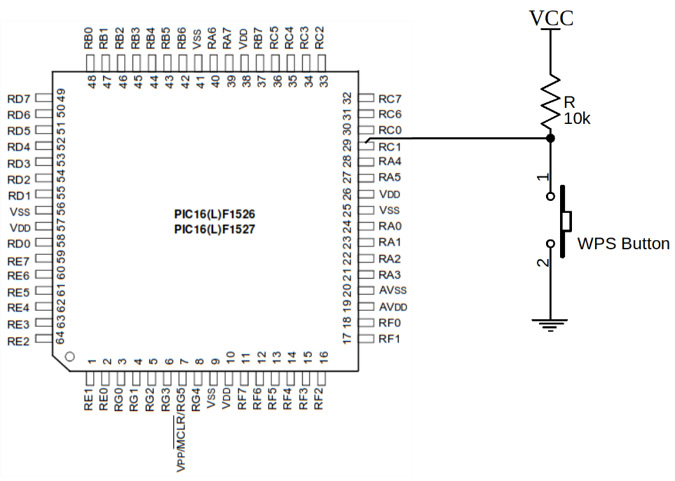
It’s rather straightforward. When the button is not pressed, the GPIO RC1 connected to the PIC is pulled to VCC, making a logic high level. As soon as the button is pressed, the pin is tied to ground, making a logic low level.
On the firmware side, handling such an input could be done in two ways: with interrupts, or by polling the GPIO state. Here, the former is done.
At each iteration of its main loop, the firmware will check the state of the RC1 input. This is done by reading the peripheral register PORTC and checking whether the bit 1 is set or not. When the button is not pressed, the bit is ‘1’ and when the button is pressed, it’s ‘0’.
Here, the RC1 is configured as an input. It’s possible to configure it as an output by unsetting the bit 1 of the TRISC peripheral register. If we set this bit, the PORTC becomes ‘0’ even though the button isn’t pressed. The value of TRISC is configured by the firmware at boot and only one time.
That’s very interesting for us, as it means if we can find a way to flip the bit 1 of the TRISC register, the firmware will actually believe the WPS button is pressed!
I’ve found a RF4CE payload able to do this. Again, it only works with one of the firmware revisions, but it doesn’t mean other firmwares aren’t exploitable, as a buffer overflow is still possible.
The Payload
The payload is shown in this table.
I’ve decomposed it into multiple sections, I’m now going to explain.
| Payload Index | Memory Address | Memory Type | Value |
|---|---|---|---|
| 0x00 | 0x3AA | General Purpose Reg | 0x00 |
| 0x01 | 0x3AB | General Purpose Reg | 0x12 |
| 0x02 | 0x3AC | General Purpose Reg | 0xC8 |
| 0x03 | 0x3AD | General Purpose Reg | 0xC0 |
| 0x04 | 0x3AE | General Purpose Reg | 0xFF |
| 0x05 | 0x3AF | General Purpose Reg | 0xCD |
| 0x06 | 0x3B0 | General Purpose Reg | 0xBB |
| 0x07 | 0x3B1 | General Purpose Reg | 0xBB |
| 0x08 | 0x3B2 | General Purpose Reg | 0xBB |
| 0x09 | 0x3B3 | General Purpose Reg | 0xBB |
| [...] | |||
| 0x43 | 0x3ED | General Purpose Reg | 0xBB |
| 0x44 | 0x3EE | General Purpose Reg | 0xBB |
| 0x45 | 0x3EF | General Purpose Reg | 0xBB |
| 0x46 | 0x3F0 | Common RAM | 0xBB |
| 0x47 | 0x3F1 | Common RAM | 0xBB |
| 0x48 | 0x3F2 | Common RAM | 0xBB |
| [...] | |||
| 0x54 | 0x3FE | Common RAM | 0xBB |
| 0x55 | 0x3FF | Common RAM | 0xBB |
| 0x56 | 0x300 | Core reg: INDF0 | 0xBB |
| 0x57 | 0x301 | Core reg: INDF1 | 0xBB |
| 0x58 | 0x302 | Core reg: PCL | 0x37 |
| 0x59 | 0x3A3 | General Purpose Reg | 0x00 |
| 0x5A | 0x3A4 | General Purpose Reg | 0x00 |
| 0x5B | 0x3A5 | General Purpose Reg | 0x00 |
| 0x5C | 0x3A6 | General Purpose Reg | 0x00 |
| 0x5D | 0x3A7 | General Purpose Reg | 0x00 |
| 0x5E | 0x3A8 | General Purpose Reg | 0x00 |
| 0x5F | 0x3A9 | General Purpose Reg | 0x00 |
The first part, ranging from 0x00 to 0x05, contains some values that cannot be explained for now, but that you will soon understand. These values are written at the expected memory addresses, starting from 0x3AA.
Next, ranging from 0x06 to 0x45, is padding. The goal here is just to increase the value of the data buffer pointer.
From index 0x46, the overflow has started. Data is now written into the Common RAM. This is actually not very useful. Padding bytes are still used.
From index 0x56, serious things are starting. The Core Registers are finally overwritten. The PCL register is set to 0x37. As the PCLATH register is equals to 0x03 in the context of the SPI_transmit function, the PIC will jump to the instruction located at 0x0337.
The code at this address is the following.
0x00000336 9231movlp0x12 >>>>> 0x00000337 b822call0x2b8 ;should call 0x12b8 when pclath=0x12 0x00000338 8331movlp0x3
There’s a function call. Nevertheless, to jump to the beginning of a valid function, the PCLATH register is expected to be set to 0x12. For us, it’s still equal to 0x03. It means the PIC will actually jump to an entirely different address, in the middle of another function.
From here, the PIC will execute dozens of instructions a jump around a couple of times. Executing all these instructions fortunately has no noticeable side effects. Finally, the following piece of code is executed.
0x000012a3 a500movwf0x25 0x000012a4 a030movlw0xa0 0x000012a5 4226call0x642 ;Read some more data from SPI bus 0x000012a6 9231movlp0x12 0x000012a7 3f08movf0x3f, w 0x000012a8 b200movwf0x32 ;dest_low 0x000012a9 a430movlw0xa4 0x000012aa b301clr0x33, f ;dest_high 0x000012ab b400movwf0x34 ;src_low 0x000012ac 0330movlw0x3 0x000012ad b500movwf0x35 ;src_high 0x000012ae 3e08movf0x3e, w ;size 0x000012af b600movwf0x36 0x000012b0 b701clr0x37, f 0x000012b1 d726call0x6d7 ;"memcpy" 0x000012b2 2700movlb0x7 0x000012b3 2308movf0x23, w 0x000012b4 0800return
A piece of code reading more bytes from the SPI bus is first called. A fixed number of 7 bytes will be read and written at addresses starting at 0x3a3 (this code is actually the one responsible for reading the very beginning of the SPI data sent by the CC2534).
Next, there’s an interesting call to the memcpy function.
The source address is set to 0x3a4. If you look carefully at the previous table, you’ll see we can control a large chuck of the data starting at 0x3a4.
The MSB of the destination address is set to 0x00 while I’ve found the low byte, set from address 0x32, to be equal to 0x83.
Thanks to another strike of luck, The size parameter can be controlled as well. For a reason I haven’t really tried to explain, this parameter is loaded with one of the bytes of the previously sent RF4CE packet. For instance, sending a stupid payload like 0c0c0c0c0c0c0c0c0c0c0c0c0c before sending the packet exploiting the overflow will ensure the size parameter is loaded with the value 0x0c.
The following table summarizes what the memcpy does, considering a size equals to 0x0c.
| Source Memory Address | Value | Destination Memory Address | Destination Register |
|---|---|---|---|
| 0x3A4 | 0x00 | 0x083 | STATUS |
| 0x3A5 | 0x00 | 0x084 | FSR0L |
| 0x3A6 | 0x00 | 0x085 | FSR0H |
| 0x3A7 | 0x00 | 0x086 | FSR1L |
| 0x3A8 | 0x00 | 0x087 | FSR1H |
| 0x3A9 | 0x00 | 0x088 | BSR |
| 0x3AA | 0x00 | 0x089 | WREG |
| 0x3AB | 0x12 | 0x08A | PCLATH |
| 0x3AC | 0xC8 | 0x08B | INTCON |
| 0x3AD | 0xC0 | 0x08C | TRISA |
| 0x3AE | 0xFF | 0x08D | TRISB |
| 0x3AF | 0xCD | 0x08E | TRISC |
As you can see, the value of multiple core registers can be controlled. These bytes come from payload indexes ranging from 0x00 to 0x05 and 0x5a to 0x5f.
To ensure the execution can continue, special care is taken with the value of registers PCLATH and INTCON.
TRISA and TRISB are set to the same value they were set before. On the contrary, TRISC is altered to simulate a WPS button press.
A “button release” can be done by setting the bit 1 of TRISC back to ‘1’ with a similar payload.
Complete Attack Scenario
By using all this knowledge, a malicious user could gain access to a protected Wi-Fi network.
Before the vulnerabilities were fixed, the following scenario was possible.
- The attacker sniffs for RF4CE packets emitted when the victim is using the remote control of the STB. The payload of these packets is ciphered, but that enough to inject crafted packets.
- The attacker sends payloads aimed at simulating a WPS button press.
- The attacker sends a similar payload, simulating a WPS button release.
- The PIC firmware is tricked into thinking the WPS button has been physically pressed. It informs the Gateway part of the system of this event. The WPS discovery is starting.
- Thanks to WPS, the attacker can connect his own devices to the Wi-Fi network of the victim.
Conclusion
It’s interesting to notice the Linux system running on the STB really looks like it has been designed with security in mind: hardened binaries are used, isolation is enforced by LXC containers, …
Nevertheless, thanks to two vulnerabilities found in what looked liked a rather non security-critical subsystem, we saw it was actually possible to remotely trigger the WPS process.
At the time of discovery, the last PIC firmware was vulnerable to the buffer overflow, but I didn’t find a way to exploit it. A proof of concept was only possible in a previous revision. Nevertheless, a determined attacker could have waited for another release of the PIC firmware, hoping it will be possible to exploit. That’s why disclosing the vulnerabilities to the manufacturer was still important.
It has been done, and the PIC firmware has been quickly patched and deployed a couple of months ago. Thankfully, the vulnerabilities cannot be exploited anymore.